ZHCS896I May 2009 – September 2018 CC430F5133 , CC430F5135 , CC430F5137 , CC430F6125 , CC430F6126 , CC430F6127 , CC430F6135 , CC430F6137
PRODUCTION DATA.
- 1器件概述
- 2修订历史记录
- 3Device Comparison
- 4Terminal Configuration and Functions
-
5Specifications
- 5.1 Absolute Maximum Ratings
- 5.2 ESD Ratings
- 5.3 Recommended Operating Conditions
- 5.4 Active Mode Supply Current Into VCC Excluding External Current
- 5.5 Typical Characteristics – Active Mode Supply Currents
- 5.6 Low-Power Mode Supply Currents (Into VCC) Excluding External Current
- 5.7 Typical Characteristics – Low-Power Mode Supply Currents
- 5.8 Low-Power Mode With LCD Supply Currents (Into VCC) Excluding External Current
- 5.9 Thermal Resistance Characteristics, CC430F51xx
- 5.10 Thermal Resistance Characteristics, CC430F61xx
- 5.11 Digital Inputs
- 5.12 Digital Outputs
- 5.13 Typical Characteristics – Outputs, Reduced Drive Strength (PxDS.y = 0)
- 5.14 Typical Characteristics – Outputs, Full Drive Strength (PxDS.y = 1)
- 5.15 Crystal Oscillator, XT1, Low-Frequency Mode
- 5.16 Internal Very-Low-Power Low-Frequency Oscillator (VLO)
- 5.17 Internal Reference, Low-Frequency Oscillator (REFO)
- 5.18 DCO Frequency
- 5.19 PMM, Brownout Reset (BOR)
- 5.20 PMM, Core Voltage
- 5.21 PMM, SVS High Side
- 5.22 PMM, SVM High Side
- 5.23 PMM, SVS Low Side
- 5.24 PMM, SVM Low Side
- 5.25 Wake-up Times From Low-Power Modes and Reset
- 5.26 Timer_A
- 5.27 USCI (UART Mode) Clock Frequency
- 5.28 USCI (UART Mode)
- 5.29 USCI (SPI Master Mode) Clock Frequency
- 5.30 USCI (SPI Master Mode)
- 5.31 USCI (SPI Slave Mode)
- 5.32 USCI (I2C Mode)
- 5.33 LCD_B Operating Conditions
- 5.34 LCD_B Electrical Characteristics
- 5.35 12-Bit ADC, Power Supply and Input Range Conditions
- 5.36 12-Bit ADC, Timing Parameters
- 5.37 12-Bit ADC, Linearity Parameters Using an External Reference Voltage or AVCC as Reference Voltage
- 5.38 12-Bit ADC, Linearity Parameters Using the Internal Reference Voltage
- 5.39 12-Bit ADC, Temperature Sensor and Built-In VMID
- 5.40 REF, External Reference
- 5.41 REF, Built-In Reference
- 5.42 Comparator_B
- 5.43 Flash Memory
- 5.44 JTAG and Spy-Bi-Wire Interface
- 5.45
RF1A CC1101-Based Radio Parameters
- 5.45.1 Recommended Operating Conditions
- 5.45.2 RF Crystal Oscillator, XT2
- 5.45.3 Current Consumption, Reduced-Power Modes
- 5.45.4 Current Consumption, Receive Mode
- 5.45.5 Current Consumption, Transmit Mode
- 5.45.6 Typical TX Current Consumption, 315 MHz
- 5.45.7 Typical TX Current Consumption, 433 MHz
- 5.45.8 Typical TX Current Consumption, 868 MHz
- 5.45.9 Typical TX Current Consumption, 915 MHz
- 5.45.10 RF Receive, Overall
- 5.45.11 RF Receive, 315 MHz
- 5.45.12 RF Receive, 433 MHz
- 5.45.13 RF Receive, 868 or 915 MHz
- 5.45.14 Typical Sensitivity, 315 MHz, Sensitivity Optimized Setting
- 5.45.15 Typical Sensitivity, 433 MHz, Sensitivity Optimized Setting
- 5.45.16 Typical Sensitivity, 868 MHz, Sensitivity Optimized Setting
- 5.45.17 Typical Sensitivity, 915 MHz, Sensitivity Optimized Setting
- 5.45.18 RF Transmit
- 5.45.19 Optimum PATABLE Settings for Various Output Power Levels and Frequency Bands
- 5.45.20 Typical Output Power, 315 MHz
- 5.45.21 Typical Output Power, 433 MHz
- 5.45.22 Typical Output Power, 868 MHz
- 5.45.23 Typical Output Power, 915 MHz
- 5.45.24 Frequency Synthesizer Characteristics
- 5.45.25 Typical RSSI_offset Values
-
6Detailed Description
- 6.1 Sub-1 GHz Radio
- 6.2 CPU
- 6.3 Operating Modes
- 6.4 Interrupt Vector Addresses
- 6.5 Memory Organization
- 6.6 Bootloader (BSL)
- 6.7 JTAG Operation
- 6.8 Flash Memory
- 6.9 RAM
- 6.10
Peripherals
- 6.10.1 Oscillator and System Clock
- 6.10.2 Power-Management Module (PMM)
- 6.10.3 Digital I/O
- 6.10.4 Port Mapping Controller
- 6.10.5 System Module (SYS)
- 6.10.6 DMA Controller
- 6.10.7 Watchdog Timer (WDT_A)
- 6.10.8 CRC16
- 6.10.9 Hardware Multiplier
- 6.10.10 AES128 Accelerator
- 6.10.11 Universal Serial Communication Interface (USCI)
- 6.10.12 TA0
- 6.10.13 TA1
- 6.10.14 Real-Time Clock (RTC_A)
- 6.10.15 Voltage Reference (REF)
- 6.10.16 LCD_B (Only CC430F613x and CC430F612x)
- 6.10.17 Comparator_B
- 6.10.18 ADC12_A (Only CC430F613x and CC430F513x)
- 6.10.19 Embedded Emulation Module (EEM) (S Version)
- 6.10.20 Peripheral File Map
- 6.11
Input/Output Diagrams
- 6.11.1 Port P1 (P1.0 to P1.4) Input/Output With Schmitt Trigger
- 6.11.2 Port P1 (P1.5 to P1.7) Input/Output With Schmitt Trigger
- 6.11.3 Port P2 (P2.0 to P2.7) Input/Output With Schmitt Trigger
- 6.11.4 Port P3 (P3.0 to P3.7) Input/Output With Schmitt Trigger
- 6.11.5 Port P4 (P4.0 to P4.7) Input/Output With Schmitt Trigger (CC430F613x and CC430F612x Only)
- 6.11.6 Port P5 (P5.0 and P5.1) Input/Output With Schmitt Trigger
- 6.11.7 Port P5 (P5.2 to P5.4) Input/Output With Schmitt Trigger (CC430F613x and CC430F612x Only)
- 6.11.8 Port P5 (P5.5 to P5.7) Input/Output With Schmitt Trigger (CC430F613x and CC430F612x Only)
- 6.11.9 Port J (PJ.0) JTAG Pin TDO, Input/Output With Schmitt Trigger or Output
- 6.11.10 Port J (PJ.1 to PJ.3) JTAG Pins TMS, TCK, TDI/TCLK, Input/Output With Schmitt Trigger or Output
- 6.12 Device Descriptor
- 7Applications, Implementation, and Layout
- 8器件和文档支持
- 9机械,封装和可订购信息
6.11.3 Port P2 (P2.0 to P2.7) Input/Output With Schmitt Trigger
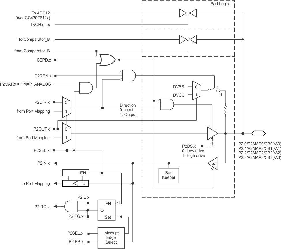
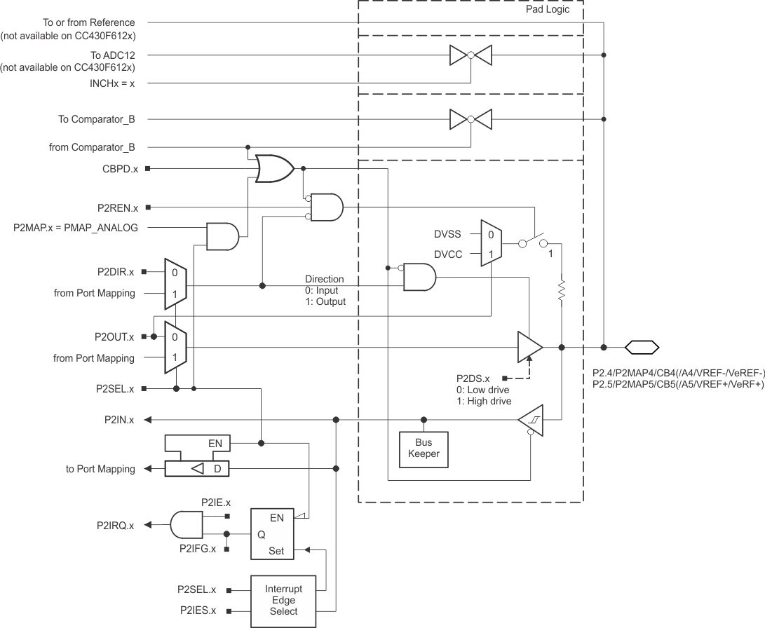
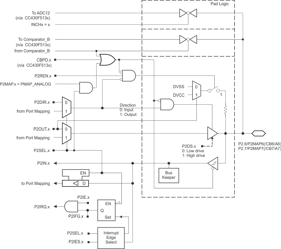
Figure 6-4 through Figure 6-6 show the port diagrams. Table 6-47 summarizes the selection of the pin functions.
 Figure 6-4 Port P2 (P2.0 to P2.3) Diagram
  Figure 6-5 Port P2 (P2.4 and P2.5) Diagram
CC430F513x devices do not provide analog functionality on port P2.6 and P2.7 pins.
Figure 6-6 Port P2 (P2.6 and P2.7) Diagram Table 6-47 Port P2 (P2.0 to P2.7) Pin Functions
| PIN NAME (P2.x) | x | FUNCTION | CONTROL BITS OR SIGNALS(1) | |||
|---|---|---|---|---|---|---|
| P2DIR.x | P2SEL.x | P2MAPx | CBPD.x | |||
| P2.0/P2MAP0/CB0 (/A0) | 0 | P2.0 (I/O) | I: 0; O: 1 | 0 | X | 0 |
| Mapped secondary digital function – see Table 6-6 | 0; 1(3) | 1 | ≤ 30(3) | 0 | ||
| A0 (not available on CC430F612x)(1) | X | 1 | = 31 | X | ||
| CB0(2) | X | X | X | 1 | ||
| P2.1/P2MAP1/CB1 (/A1) | 1 | P2.1 (I/O) | I: 0; O: 1 | 0 | X | 0 |
| Mapped secondary digital function – see Table 6-6 | 0; 1(3) | 1 | ≤ 30(3) | 0 | ||
| A1 (not available on CC430F612x)(1) | X | 1 | = 31 | X | ||
| CB1(2) | X | X | X | 1 | ||
| P2.2/P2MAP2/CB2 (/A2) | 2 | P2.2 (I/O) | I: 0; O: 1 | 0 | X | 0 |
| Mapped secondary digital function – see Table 6-6 | 0; 1(3) | 1 | ≤ 30(3) | 0 | ||
| A2 (not available on CC430F612x)(1) | X | 1 | = 31 | X | ||
| CB2(2) | X | X | X | 1 | ||
| P2.3/P2MAP3/CB3 (/A3) | 3 | P2.3 (I/O) | I: 0; O: 1 | 0 | X | 0 |
| Mapped secondary digital function – see Table 6-6 | 0; 1(3) | 1 | ≤ 30(3) | 0 | ||
| A3 (not available on CC430F612x)(1) | X | 1 | = 31 | X | ||
| CB3(2) | X | X | X | 1 | ||
| P2.4/P2MAP4/CB4 (/A4/VREF-/VeREF-) | 4 | P2.4 (I/O) | I: 0; O: 1 | 0 | X | 0 |
| Mapped secondary digital function – see Table 6-6 | 0; 1(3) | 1 | ≤ 30(3) | 0 | ||
| A4/VREF-/VeREF- (not available on CC430F612x)(1) | X | 1 | = 31 | X | ||
| CB4(2) | X | X | X | 1 | ||
| P2.5/P2MAP5/CB5 (/A5/VREF+/VeREF+) | 5 | P2.5 (I/O) | I: 0; O: 1 | 0 | X | 0 |
| Mapped secondary digital function – see Table 6-6 | 0; 1(3) | 1 | ≤ 30(3) | 0 | ||
| A5/VREF+/VeREF+ (not available on CC430F612x)(1) | X | 1 | = 31 | X | ||
| CB5(2) | X | X | X | 1 | ||
| P2.6/P2MAP6(/CB6) (/A6) | 6 | P2.6 (I/O) | I: 0; O: 1 | 0 | X | 0 |
| Mapped secondary digital function – see Table 6-6 | 0; 1(3) | 1 | ≤ 30(3) | 0 | ||
| A6 (not available on CC430F612x and CC430F513x)(1) | X | 1 | = 31 | X | ||
| CB6 (not available on CC430F513x)(2) | X | X | X | 1 | ||
| P2.7/P2MAP7(/CB7) (/A7) | 7 | P2.7 (I/O) | I: 0; O: 1 | 0 | X | 0 |
| Mapped secondary digital function – see Table 6-6 | 0; 1(3) | 1 | ≤ 30(3) | 0 | ||
| A7 (not available on CC430F612x and CC430F513x)(1) | X | 1 | = 31 | X | ||
| CB7 (not available on CC430F513x)(2) | X | X | X | 1 | ||
(1) Setting P2SEL.x bit together with P2MAPx = PM_ANALOG disables the output driver and the input Schmitt trigger.
(2) Setting the CBPD.x bit disables the output driver and the input Schmitt trigger to prevent parasitic cross currents when applying analog signals. Selecting the CBx input pin to the comparator multiplexer with the CBx bits automatically disables output driver and input buffer for that pin, regardless of the state of the associated CBPD.x bit.