ZHCS994B June 2012 – September 2018 CC430F5123 , CC430F5125 , CC430F5143 , CC430F5145 , CC430F5147 , CC430F6147
PRODUCTION DATA.
- 1器件概述
- 2修订历史记录
- 3Device Comparison
- 4Terminal Configuration and Functions
-
5Specifications
- 5.1 Absolute Maximum Ratings
- 5.2 ESD Ratings
- 5.3 Recommended Operating Conditions
- 5.4 Active Mode Supply Current Into VCC Excluding External Current
- 5.5 Typical Characteristics – Active Mode Supply Currents
- 5.6 Low-Power Mode Supply Currents (Into VCC) Excluding External Current
- 5.7 Typical Characteristics – Low-Power Mode Supply Currents
- 5.8 Low-Power Mode With LCD Supply Currents (Into VCC) Excluding External Current
- 5.9 Thermal Resistance Characteristics, CC430F51xx
- 5.10 Thermal Resistance Characteristics, CC430F61xx
- 5.11 Digital Inputs
- 5.12 Digital Outputs
- 5.13 Typical Characteristics – Outputs, Reduced Drive Strength (PxDS.y = 0)
- 5.14 Typical Characteristics – Outputs, Full Drive Strength (PxDS.y = 1)
- 5.15 Crystal Oscillator, XT1, Low-Frequency Mode
- 5.16 Internal Very-Low-Power Low-Frequency Oscillator (VLO)
- 5.17 Internal Reference, Low-Frequency Oscillator (REFO)
- 5.18 DCO Frequency
- 5.19 PMM, Brownout Reset (BOR)
- 5.20 PMM, Core Voltage
- 5.21 PMM, SVS High Side
- 5.22 PMM, SVM High Side
- 5.23 PMM, SVS Low Side
- 5.24 PMM, SVM Low Side
- 5.25 Wake-up Times From Low-Power Modes and Reset
- 5.26 Timer_A
- 5.27 USCI (UART Mode) Clock Frequency
- 5.28 USCI (UART Mode)
- 5.29 USCI (SPI Master Mode) Clock Frequency
- 5.30 USCI (SPI Master Mode)
- 5.31 USCI (SPI Slave Mode)
- 5.32 USCI (I2C Mode)
- 5.33 LCD_B Operating Conditions
- 5.34 LCD_B Electrical Characteristics
- 5.35 10-Bit ADC, Power Supply and Input Range Conditions
- 5.36 10-Bit ADC, Timing Parameters
- 5.37 10-Bit ADC, Linearity Parameters
- 5.38 REF, External Reference
- 5.39 REF, Built-In Reference
- 5.40 Comparator_B
- 5.41 Flash Memory
- 5.42 JTAG and Spy-Bi-Wire Interface
- 5.43
RF1A CC1101-Based Radio Parameters
- 5.43.1 RF1A Recommended Operating Conditions
- 5.43.2 RF Crystal Oscillator, XT2
- 5.43.3 Current Consumption, Reduced-Power Modes
- 5.43.4 Current Consumption, Receive Mode
- 5.43.5 Current Consumption, Transmit Mode
- 5.43.6 Typical TX Current Consumption, 315 MHz, 25°C
- 5.43.7 Typical TX Current Consumption, 433 MHz, 25°C
- 5.43.8 Typical TX Current Consumption, 868 MHz
- 5.43.9 Typical TX Current Consumption, 915 MHz
- 5.43.10 RF Receive, Overall
- 5.43.11 RF Receive, 315 MHz
- 5.43.12 RF Receive, 433 MHz
- 5.43.13 RF Receive, 868 MHz and 915 MHz
- 5.43.14 Typical Sensitivity, 315 MHz, Sensitivity Optimized Setting
- 5.43.15 Typical Sensitivity, 433 MHz, Sensitivity Optimized Setting
- 5.43.16 Typical Sensitivity, 868 MHz, Sensitivity Optimized Setting
- 5.43.17 Typical Sensitivity, 915 MHz, Sensitivity Optimized Setting
- 5.43.18 RF Transmit
- 5.43.19 Optimum PATABLE Settings for Various Output Power Levels and Frequency Bands
- 5.43.20 Typical Output Power, 315 MHz
- 5.43.21 Typical Output Power, 433 MHz
- 5.43.22 Typical Output Power, 868 MHz
- 5.43.23 Typical Output Power, 915 MHz
- 5.43.24 Frequency Synthesizer Characteristics
- 5.43.25 Typical RSSI_offset Values
-
6Detailed Description
- 6.1 Sub-1 GHz Radio
- 6.2 CPU
- 6.3 Operating Modes
- 6.4 Interrupt Vector Addresses
- 6.5 Memory Organization
- 6.6 Bootloader (BSL)
- 6.7 JTAG Operation
- 6.8 Flash Memory
- 6.9 RAM
- 6.10 Backup RAM
- 6.11
Peripherals
- 6.11.1 Oscillator and System Clock
- 6.11.2 Power-Management Module (PMM)
- 6.11.3 Digital I/O
- 6.11.4 Port Mapping Controller
- 6.11.5 System Module (SYS)
- 6.11.6 DMA Controller
- 6.11.7 Watchdog Timer (WDT_A)
- 6.11.8 CRC16
- 6.11.9 Hardware Multiplier
- 6.11.10 AES128 Accelerator
- 6.11.11 Universal Serial Communication Interface (USCI)
- 6.11.12 TA0
- 6.11.13 TA1
- 6.11.14 Real-Time Clock (RTC_D)
- 6.11.15 Voltage Reference (REF) (Including Output)
- 6.11.16 LCD_B (Only CC430F614x)
- 6.11.17 Comparator_B
- 6.11.18 ADC10_A (CC430F614x and CC430F514x Only)
- 6.11.19 Embedded Emulation Module (EEM) (S Version)
- 6.11.20 Peripheral File Map
- 6.12
Input/Output Diagrams
- 6.12.1 Port P1 (P1.0 to P1.4) Input/Output With Schmitt Trigger
- 6.12.2 Port P1 (P1.5 to P1.7) Input/Output With Schmitt Trigger
- 6.12.3 Port P2 (P2.0 to P2.7) Input/Output With Schmitt Trigger
- 6.12.4 Port P3 (P3.0 to P3.7) Input/Output With Schmitt Trigger
- 6.12.5 Port P4 (P4.0 to P4.7) Input/Output With Schmitt Trigger (CC430F614x Only)
- 6.12.6 Port P5 (P5.0 and P5.1) Input/Output With Schmitt Trigger
- 6.12.7 Port P5 (P5.2 to P5.4) Input/Output With Schmitt Trigger (CC430F614x Only)
- 6.12.8 Port P5 (P5.5 to P5.7) Input/Output With Schmitt Trigger (CC430F614x Only)
- 6.12.9 Port PJ (PJ.0) JTAG Pin TDO, Input/Output With Schmitt Trigger or Output
- 6.12.10 Port PJ (PJ.1 to PJ.3) JTAG Pins TMS, TCK, TDI/TCLK, Input/Output With Schmitt Trigger or Output
- 6.13 Device Descriptor Structure
- 7Applications, Implementation, and Layout
- 8器件和文档支持
- 9机械,封装和可订购信息
5.30 USCI (SPI Master Mode)
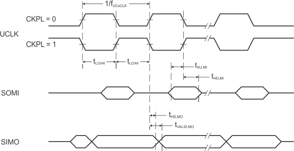
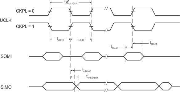
over recommended ranges of supply voltage and operating free-air temperature (unless otherwise noted)(1) (see Figure 5-16 and Figure 5-17)| PARAMETER | TEST CONDITIONS | PMMCOREVx | VCC | MIN | MAX | UNIT | |
|---|---|---|---|---|---|---|---|
| tSU,MI | SOMI input data setup time | 0 | 1.8 V | 55 | ns | ||
| 3 V | 38 | ||||||
| 3 | 2.4 V | 30 | |||||
| 3 V | 25 | ||||||
| tHD,MI | SOMI input data hold time | 0 | 1.8 V | 0 | ns | ||
| 3 V | 0 | ||||||
| 3 | 2.4 V | 0 | |||||
| 3 V | 0 | ||||||
| tVALID,MO | SIMO output data valid time(2) | UCLK edge to SIMO valid,
CL = 20 pF |
0 | 1.8 V | 20 | ns | |
| 3 V | 18 | ||||||
| 3 | 2.4 V | 16 | |||||
| 3 V | 15 | ||||||
| tHD,MO | SIMO output data hold time(3) | CL = 20 pF | 0 | 1.8 V | –10 | ns | |
| 3 V | –8 | ||||||
| 3 | 2.4 V | –10 | |||||
| 3 V | –8 | ||||||
(1) fUCxCLK = 1/2tLO/HI with tLO/HI ≥ max(tVALID,MO(USCI) + tSU,SI(Slave), tSU,MI(USCI) + tVALID,SO(Slave))
For the slave parameters tSU,SI(Slave) and tVALID,SO(Slave), see the SPI parameters of the attached slave.
For the slave parameters tSU,SI(Slave) and tVALID,SO(Slave), see the SPI parameters of the attached slave.
(2) Specifies the time to drive the next valid data to the SIMO output after the output changing UCLK clock edge. See the timing diagrams in Figure 5-16 and Figure 5-17.
(3) Specifies how long data on the SIMO output is valid after the output changing UCLK clock edge. Negative values indicate that the data on the SIMO output can become invalid before the output changing clock edge observed on UCLK. See the timing diagrams in Figure 5-16 and Figure 5-17.
 Figure 5-16 SPI Master Mode, CKPH = 0
  Figure 5-17 SPI Master Mode, CKPH = 1