SCHS097F November 1998 – March 2017 CD40106B
PRODUCTION DATA.
- 1 Features
- 2 Applications
- 3 Description
- 4 Revision History
- 5 Pin Configuration and Functions
- 6 Specifications
- 7 Parameter Measurement Information
- 8 Detailed Description
- 9 Application and Implementation
- 10Power Supply Recommendations
- 11Layout
- 12Device and Documentation Support
- 13Mechanical, Packaging, and Orderable Information
封装选项
机械数据 (封装 | 引脚)
散热焊盘机械数据 (封装 | 引脚)
订购信息
9 Application and Implementation
NOTE
Information in the following applications sections is not part of the TI component specification, and TI does not warrant its accuracy or completeness. TI’s customers are responsible for determining suitability of components for their purposes. Customers should validate and test their design implementation to confirm system functionality.
9.1 Application Information
The CD40106B device is a Schmitt-Trigger input device that can be used for a multitude of inverting buffer type functions. The application shown here takes advantage of the Schmitt-Trigger inputs to produce a square wave output from a sine wave input.
9.2 Typical Applications
9.2.1 Wave Shaper
 Figure 17. Wave Shaper Schematic
9.2.1.1 Design Requirements
Take care to avoid bus contention, because it can drive currents that would exceed maximum limits. Parallel output drive can create fast edges into light loads so consider routing and load conditions to prevent ringing.
9.2.1.2 Detailed Design Procedure
The recommended input conditions for Figure 17 includes specified high and low levels (see VP and VN in Electrical Characteristics: Static). Inputs are not overvoltage tolerant and must be below VCC level because of the presence of input clamp diodes to VCC.
The recommended output condition for the CD40106B application includes specific load currents. Load currents must be limited so as to not exceed the total power (continuous current through VCC or GND) for the device. These limits are in the Absolute Maximum Ratings. Outputs must not be pulled above VCC.
9.2.1.3 Application Curve
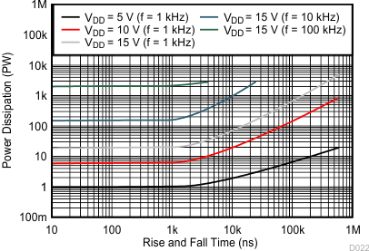
 Figure 18. Typical Power Dissipation as a Function of Rise and Fall Times
9.2.2 Monostable Multivibrator
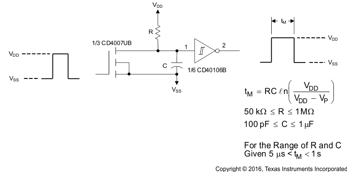
The timing of the monostable multivibrator circuit can be set by following the equations shown in Figure 19.
 Figure 19. Monostable Multivibrator Schematic and Equations
9.2.3 Astable Multivibrator
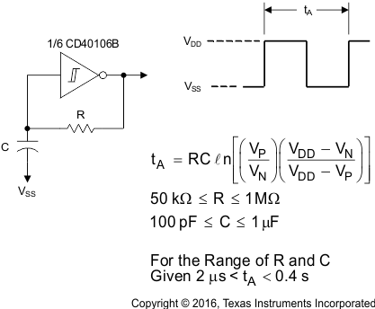
The timing of the astable multivibrator circuit can be set by following the equations shown in Figure 20.
 Figure 20. Astable Multivibrator Schematic and Equations