SCHS023E November 1998 – September 2016 CD4013B
PRODUCTION DATA.
6 Specifications
6.1 Absolute Maximum Ratings
over operating free-air temperature range (unless otherwise noted)(1)| MIN | MAX | UNIT | ||
|---|---|---|---|---|
| DC supply voltage, VDD(2) | –0.5 | 20 | V | |
| Input voltage, all inputs | –0.5 | VDD + 0.5 | V | |
| DC input current, any one input | 10 | mA | ||
| Power dissipation, PD | TA = –55°C to 100°C | 500 | mW | |
| TA = 100°C to 125°C(3) | 200 | |||
| Device dissipation per output transistor | 100 | mW | ||
| Operating temperature, TA | –55 | 125 | °C | |
| Storage temperature, Tstg | –65 | 150 | °C | |
(1) Stresses beyond those listed under Absolute Maximum Ratings may cause permanent damage to the device. These are stress ratings only, which do not imply functional operation of the device at these or any other conditions beyond those indicated under Recommended Operating Conditions. Exposure to absolute-maximum-rated conditions for extended periods may affect device reliability.
(2) Voltages reference to VSS terminal
(3) Derate linearity at 12 mW/°C
6.2 ESD Ratings
| VALUE | UNIT | |||
|---|---|---|---|---|
| V(ESD) | Electrostatic discharge | Human-body model (HBM), per ANSI/ESDA/JEDEC JS-001(1) | ±2000 | V |
| Charged-device model (CDM), per JEDEC specification JESD22-C101(2) | ±1000 | |||
(1) JEDEC document JEP155 states that 500-V HBM allows safe manufacturing with a standard ESD control process.
(2) JEDEC document JEP157 states that 250-V CDM allows safe manufacturing with a standard ESD control process.
6.3 Recommended Operating Conditions
over operating free-air temperature range (unless otherwise noted)| MIN | TYP | MAX | UNIT | |||
|---|---|---|---|---|---|---|
| Supply voltage | 3 | 18 | V | |||
| tS | Data setup time | VDD = 5 | 40 | ns | ||
| VDD = 10 | 20 | |||||
| VDD = 15 | 15 | |||||
| tW | Clock pulse width | VDD = 5 | 140 | ns | ||
| VDD = 10 | 60 | |||||
| VDD = 15 | 40 | |||||
| fCL | Clock input frequency | VDD = 5 | 3.5 | 7 | MHz | |
| VDD = 10 | 8 | 16 | ||||
| VDD = 15 | 12 | 24 | ||||
| trCL(1)
tfCL |
Clock rise or fall time | VDD = 5 | 15 | µs | ||
| VDD = 10 | 10 | |||||
| VDD = 15 | 5 | |||||
| tW | Set or reset pulse width | VDD = 5 | 180 | ns | ||
| VDD = 10 | 80 | |||||
| VDD = 15 | 50 | |||||
(1) If more than one unit is cascaded in a parallel clocked operation, trCL must be made less than or equal to the sum of the fixed propagation delay time at 15 pF and the transistion time of the output driving stage for the estimated capacitive load.
6.4 Thermal Information
| THERMAL METRIC(1) | CD4013B | UNIT | ||||
|---|---|---|---|---|---|---|
| N (PDIP) | D (SOIC) | NS (SO) | PW (TSSOP) | |||
| 14 PINS | 14 PINS | 14 PINS | 14 PINS | |||
| RθJA | Junction-to-ambient thermal resistance | 47.1 | 92.5 | 89.3 | 121 | °C/W |
| RθJC(top) | Junction-to-case (top) thermal resistance | 34.5 | 54 | 47.1 | 49.6 | °C/W |
| RθJB | Junction-to-board thermal resistance | 27.1 | 46.8 | 48 | 62.7 | °C/W |
| ψJT | Junction-to-top characterization parameter | 19.4 | 19 | 17 | 5.9 | °C/W |
| ψJB | Junction-to-board characterization parameter | 27 | 46.5 | 47.7 | 62.1 | °C/W |
(1) For more information about traditional and new thermal metrics, see the Semiconductor and IC Package Thermal Metrics application report.
6.5 Electrical Characteristics: Static
over operating free-air temperature range (unless otherwise noted)| PARAMETER | TEST CONDITIONS | MIN | TYP | MAX | UNIT | ||
|---|---|---|---|---|---|---|---|
| IDDmax | Quiescent device current | VIN = 0 or 5, VDD = 5 | TA = –55°C | 1 | µA | ||
| TA = –40°C | 1 | ||||||
| TA = 25°C | 0.02 | 1 | |||||
| TA = 85°C | 30 | ||||||
| TA = 125°C | 30 | ||||||
| VIN = 0 or 10, VDD = 10 | TA = –55°C | 2 | |||||
| TA = –40°C | 2 | ||||||
| TA = 25°C | 0.02 | 2 | |||||
| TA = 85°C | 60 | ||||||
| TA = 125°C | 60 | ||||||
| VIN = 0 or 15, VDD = 15 | TA = –55°C | 4 | |||||
| TA = –40°C | 4 | ||||||
| TA = 25°C | 0.02 | 4 | |||||
| TA = 85°C | 120 | ||||||
| TA = 125°C | 120 | ||||||
| VIN = 0 or 20, VDD = 20 | TA = –55°C | 20 | |||||
| TA = –40°C | 20 | ||||||
| TA = 25°C | 0.04 | 20 | |||||
| TA = 85°C | 600 | ||||||
| TA = 125°C | 600 | ||||||
| IOLmin | Output low (sink) current | VO = 0.4, VIN = 0 or 5, VDD = 5 |
TA = –55°C | 0.64 | mA | ||
| TA = –40°C | 0.61 | ||||||
| TA = 25°C | 0.51 | 1 | |||||
| TA = 85°C | 0.42 | ||||||
| TA = 125°C | 0.36 | ||||||
| VO = 0.5, VIN = 0 or 10, VDD = 10 |
TA = –55°C | 1.6 | |||||
| TA = –40°C | 1.5 | ||||||
| TA = 25°C | 1.3 | 2.6 | |||||
| TA = 85°C | 1.1 | ||||||
| TA = 125°C | 0.9 | ||||||
| VO = 1.5, VIN = 0 or 15, VDD = 15 |
TA = –55°C | 4.2 | |||||
| TA = –40°C | 4 | ||||||
| TA = 25°C | 3.4 | 6.8 | |||||
| TA = 85°C | 2.8 | ||||||
| TA = 125°C | 2.4 | ||||||
| IOHmin | Output high (source) current | VO = 4.6, VIN = 0 or 5, VDD = 5 |
TA = –55°C | –0.64 | mA | ||
| TA = –40°C | –0.61 | ||||||
| TA = 25°C | –0.51 | –1 | |||||
| TA = 85°C | –0.42 | ||||||
| TA = 125°C | –0.36 | ||||||
| VO = 2.5, VIN = 0 or 5, VDD = 5 |
TA = –55°C | –2 | |||||
| TA = –40°C | –1.8 | ||||||
| TA = 25°C | –1.6 | –3.2 | |||||
| TA = 85°C | –1.3 | ||||||
| TA = 125°C | –1.15 | ||||||
| VO = 9.5, VIN = 0 or 10, VDD = 10 |
TA = –55°C | –1.6 | |||||
| TA = –40°C | –1.5 | ||||||
| TA = 25°C | –1.3 | –2.6 | |||||
| TA = 85°C | –1.1 | ||||||
| TA = 125°C | –0.9 | ||||||
| VO = 13.5, VIN = 0 or 15, VDD = 15 |
TA = –55°C | –4.2 | |||||
| TA = –40°C | –4 | ||||||
| TA = 25°C | –3.4 | –6.8 | |||||
| TA = 85°C | –2.8 | ||||||
| TA = 125°C | –2.4 | ||||||
| VOLmax | Low-level output voltage | VIN = 0 or 5, VDD = 5 | TA = –55°C, –40°C, 25°C, 85°C, and 125°C |
0 | 0.05 | V | |
| VIN = 0 or 10, VDD = 10 | TA = –55°C, –40°C, 25°C, 85°C, and 125°C |
0 | 0.05 | ||||
| VIN = 0 or 15, VDD = 15 | TA = –55°C, –40°C, 25°C, 85°C, and 125°C |
0 | 0.05 | ||||
| VOHmin | High-level output voltage | VIN = 0 or 5, VDD = 5 | TA = –55°C, –40°C, 25°C, 85°C, and 125°C |
4.95 | 5 | V | |
| VIN = 0 or 10, VDD = 10 | TA = –55°C, –40°C, 25°C, 85°C, and 125°C |
9.95 | 10 | ||||
| VIN = 0 or 15, VDD = 15 | TA = –55°C, –40°C, 25°C, 85°C, and 125°C |
14.95 | 15 | ||||
| VILmax | Input low voltage | VO = 0.5 or 4.5, VDD = 5 | TA = –55°C, –40°C, 25°C, 85°C, and 125°C |
1.5 | V | ||
| VO = 1 or 9, VDD = 10 | TA = –55°C, –40°C, 25°C, 85°C, and 125°C |
3 | |||||
| VO = 1.5 or 13.5, VDD = 15 |
TA = –55°C, –40°C, 25°C, 85°C, and 125°C |
4 | |||||
| VIHmin | Input high voltage | VO = 0.5 or 4.5, VDD = 5 | TA = –55°C, –40°C, 25°C, 85°C, and 125°C |
3.5 | V | ||
| VO = 1 or 9, VDD = 10 | TA = –55°C, –40°C, 25°C, 85°C, and 125°C |
7 | |||||
| VO = 1.5 or 13.5, VDD = 15 |
TA = –55°C, –40°C, 25°C, 85°C, and 125°C |
11 | |||||
| IINmax | Input current | VIN = 0 or 18, VDD = 18 | TA = –55°C | ±0.1 | µA | ||
| TA = –40°C | ±0.1 | ||||||
| TA = 25°C | ±10–5 | ±0.1 | |||||
| TA = 85°C | ±1 | ||||||
| TA = 125°C | ±1 | ||||||
6.6 Electrical Characteristics: Dynamic
at TA = 25°C, input tr, tf = 20 ns, CL = 50 pF, RL = 20 kΩ (unless otherwise noted)| PARAMETER | TEST CONDITIONS | MIN | TYP | MAX | UNIT | |
|---|---|---|---|---|---|---|
| tPHL, tPLH |
Propagation delay time, clock to Q or Q outputs |
VDD = 5 | 150 | 300 | ns | |
| VDD = 10 | 65 | 130 | ||||
| VDD = 15 | 45 | 90 | ||||
| tPLH | Set to Q or reset to Q | VDD = 5 | 150 | 300 | ns | |
| VDD = 10 | 65 | 130 | ||||
| VDD = 15 | 45 | 90 | ||||
| tPHL | Set to Q or reset to Q | VDD = 5 | 200 | 400 | ns | |
| VDD = 10 | 85 | 170 | ||||
| VDD = 15 | 60 | 120 | ||||
| tTHL, tTLH |
Transition time | VDD = 5 | 100 | 200 | ns | |
| VDD = 10 | 50 | 100 | ||||
| VDD = 15 | 40 | 80 | ||||
| fCL | Maximum clock input frequency(1) | VDD = 5 | 3.5 | 7 | MHz | |
| VDD = 10 | 8 | 16 | ||||
| VDD = 15 | 12 | 24 | ||||
| tW | Minimum clock pulse width | VDD = 5 | 70 | 140 | ns | |
| VDD = 10 | 30 | 60 | ||||
| VDD = 15 | 20 | 40 | ||||
| Minimum set or reset pulse width | VDD = 5 | 90 | 180 | ns | ||
| VDD = 10 | 40 | 80 | ||||
| VDD = 15 | 25 | 50 | ||||
| tS | Minimum data setup time | VDD = 5 | 20 | 40 | ns | |
| VDD = 10 | 10 | 20 | ||||
| VDD = 15 | 7 | 15 | ||||
| tH | Minimum data hold time | VDD = 5, 10, 15 | 2 | 5 | ns | |
| trCL, tfCL |
Clock input rise or fall time | VDD = 5 | 15 | µs | ||
| VDD = 10 | 10 | |||||
| VDD = 15 | 5 | |||||
| CIN | Input capacitance | Any input | 5 | 7.5 | pF | |
(1) Input tr, tf = 5 ns
6.7 Typical Characteristics
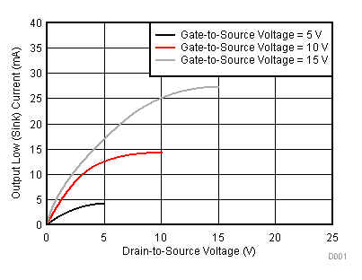 Figure 1. Typical Output Low (Sink) Current
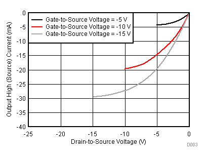 Figure 3. Typical Output High (Source) Current
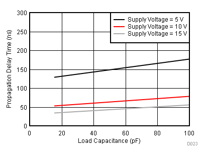
CLOCK or SET to Q, CLOCK or RESET to Q
Figure 5. Typical Propagation Delay Timevs Load Capacitance
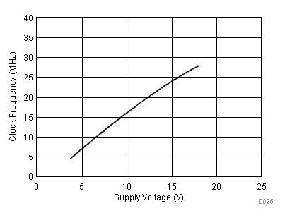 Figure 7. Typical Maximum Clock Frequency
vs Supply Voltage
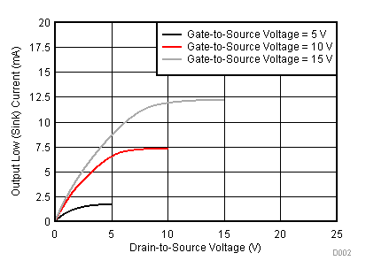 Figure 2. Minimum Output Low (Sink) Current
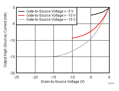 Figure 4. Minimum Output High (Source) Current
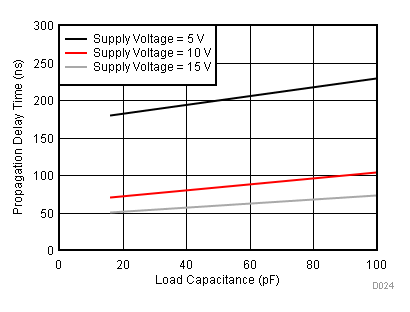
SET to Q or RESET to Q
Figure 6. Typical Propagation Delay Timevs Load Capacitance
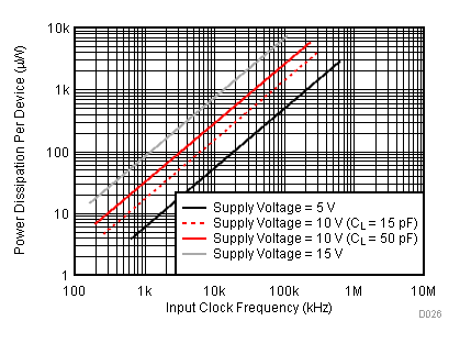 Figure 8. Typical Power Dissipation vs Frequency