ZHCSO69D November 1998 – July 2021 CD4027B
PRODUCTION DATA
5 Pin Configuration and Functions
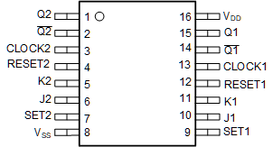
 Figure 5-1 Terminal Assignment
Table 5-1 Pin Functions
| PIN | I/O | DESCRIPTION | |
|---|---|---|---|
| NAME | NO. | ||
| CLOCK1 | 13 | I | Clock input for channel 1 |
| CLOCK2 | 3 | I | Clock input for channel 2 |
| J1 | 10 | I | J input for channel 1 |
| J2 | 6 | I | J input for channel 2 |
| K1 | 11 | I | K input for channel 1 |
| K2 | 5 | I | K input for channel 2 |
| Q1 | 15 | O | Q output for channel 1 |
| Q1 | 14 | O | Inverted Q output for channel 1 |
| Q2 | 1 | O | Q output for channel 2 |
| Q2 | 2 | O | Inverted Q output for channel 2 |
| RESET1 | 12 | I | Reset input for channel 1 |
| RESET2 | 4 | I | Reset input for channel 2 |
| SET1 | 9 | I | Set input for channel 1 |
| SET2 | 7 | I | Set input for channel 2 |
| VDD | 16 | — | Supply |
| VSS | 8 | — | Ground |