ZHCSWW3E November 1998 – August 2024 CD54AC74 , CD74AC74
PRODUCTION DATA
- 1
- 1 特性
- 2 说明
- 3 Pin Configuration and Functions
-
4 Specifications
- 4.1 Absolute Maximum Ratings
- 4.2 ESD Ratings
- 4.3 Recommended Operating Conditions
- 4.4 Thermal Information
- 4.5 Electrical Characteristics
- 4.6 Timing Requirements, VCC = 1.5 V
- 4.7 Timing Requirements, VCC = 3.3 V ± 0.3 V
- 4.8 Timing Requirements, VCC = 5 V ± 0.5 V
- 4.9 Switching Characteristics, VCC = 1.5 V
- 4.10 Switching Characteristics, VCC = 3.3 V ± 0.3 V
- 4.11 Switching Characteristics, VCC = 5 V ± 0.5 V
- 4.12 Operating Characteristics
- 5 Parameter Measurement Information
- 6 Detailed Description
- 7 Application and Implementation
- 8 Device and Documentation Support
- 9 Revision History
- 10Mechanical, Packaging, and Orderable Information
3 Pin Configuration and Functions
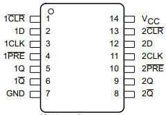
 Figure 3-1 CD54AC74 F Package, 14-Pin
CDIP; CD74AC74 E or M Package, 14-Pin PDIP or SOIC (Top View)
Figure 3-1 CD54AC74 F Package, 14-Pin
CDIP; CD74AC74 E or M Package, 14-Pin PDIP or SOIC (Top View)Pin Functions
| PIN | I/O | DESCRIPTION | |
|---|---|---|---|
| NAME | NO. | ||
| 1 CLR | 1 | Input | Channel 1, Clear Input, Active Low |
| 1D | 2 | Input | Channel 1, Data Input |
| 1CLK | 3 | Input | Channel 1, Positive edge triggered clock input |
| 1 PRE | 4 | Input | Channel 1, Preset Input, Active Low |
| 1Q | 5 | Output | Channel 1, Output |
| 1 Q | 6 | Output | Channel 1, Inverted Output |
| GND | 7 | — | Ground |
| 2 Q | 8 | Output | Channel 2, Inverted Output |
| 2Q | 9 | Output | Channel 2, Output |
| 2 PRE | 10 | Input | Channel 2, Preset Input, Active Low |
| 2CLK | 11 | Input | Channel 2, Positive edge triggered clock input |
| 2D | 12 | Input | Channel 2, Data Input |
| 2 CLR | 13 | Input | Channel 2, Clear Input, Active Low |
| VCC | 14 | — | Positive Supply |