ZHCSWW0A December 2002 – July 2024 CD54ACT74 , CD74ACT74
PRODUCTION DATA
3 Pin Configuration and Functions
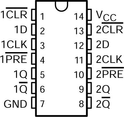
 Figure 3-1 D, N, or J Package
14-Pin SOIC, PDIP, or CDIP
(Top View)
Table 3-1 Pin Functions
| PIN | TYPE1 | DESCRIPTION | |
|---|---|---|---|
| NAME | NO. | ||
| 1CLR | 1 | I | Asynchronous clear for channel 1, active low |
| 1D | 2 | I | Data for channel 1 |
| 1CLK | 3 | I | Clock for channel 1, rising edge triggered |
| 1PRE | 4 | I | Asynchronous preset for channel 1, active low |
| 1Q | 5 | O | Output for channel 1 |
| 1Q | 6 | O | Inverted output for channel 1 |
| GND | 7 | G | Ground |
| 2Q | 8 | O | Inverted output for channel 2 |
| 2Q | 9 | O | Output for channel 2 |
| 2PRE | 10 | I | Asynchronous preset for channel 2, active low |
| 2CLK | 11 | I | Clock for channel 2, rising edge triggered |
| 2D | 12 | I | Data for channel 2 |
| 2CLR | 13 | I | Asynchronous clear for channel 2, active low |
| VCC | 14 | P | Positive supply |
- Signal Types: I = Input, O = Output, I/O = Input or Output.