ZHCSQ50E November 1998 – March 2022 CD54HC243 , CD74HC243 , CD74HCT243
PRODUCTION DATA
6 Parameter Measurement Information
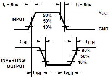
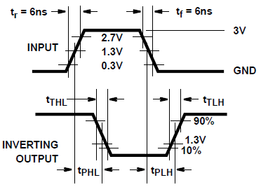
tPD is the maximum between tPLH and tPHL
tt is the maximum between tTLH and tTHL
 Figure 6-1 HC and HCT transition times and
propagation delay times, combination logic
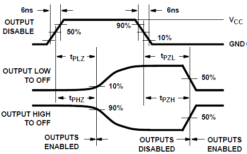
 Figure 6-3 HC three-state propagation delay
waveform
NOTE: Open drain waveforms tPLZ and tPZL are the same as those for three-state shown on the left. The test circuit is Output RL = 1kΩ to VCC, CL = 50pF.
Figure 6-5 HC and HCT three-state propagation delay test circuit Figure 6-2 HCT transition times and tpopationg
delay times, combination logic
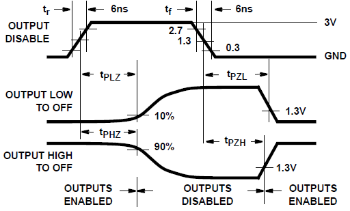
 Figure 6-4 HCT three-state propagation delay
waveform