ZHCSOB2E August   1997  – June 2021 CD54HC86 , CD74HC86

PRODUCTION DATA  

  1. 特性
  2. 应用
  3. 说明
  4. Revision History
  5. Pin Configuration and Functions
    1.     Pin Functions
  6. Specifications
    1. 6.1 Absolute Maximum Ratings
    2. 6.2 ESD Ratings
    3. 6.3 Recommended Operating Conditions
    4. 6.4 Thermal Information
    5. 6.5 Electrical Characteristics
    6. 6.6 Switching Characteristics
    7. 6.7 Operating Characteristics
    8. 6.8 Typical Characteristics
  7. Parameter Measurement Information
  8. Detailed Description
    1. 8.1 Overview
    2. 8.2 Functional Block Diagram
    3. 8.3 Feature Description
      1. 8.3.1 Balanced CMOS Push-Pull Outputs
      2. 8.3.2 Standard CMOS Inputs
      3. 8.3.3 Clamp Diode Structure
    4. 8.4 Device Functional Modes
  9. Application and Implementation
    1. 9.1 Application Information
    2. 9.2 Typical Application
      1. 9.2.1 Design Requirements
        1. 9.2.1.1 Power Considerations
        2. 9.2.1.2 Input Considerations
        3. 9.2.1.3 Output Considerations
      2. 9.2.2 Detailed Design Procedure
      3. 9.2.3 Application Curves
  10. 10Power Supply Recommendations
  11. 11Layout
    1. 11.1 Layout Guidelines
    2. 11.2 Layout Example
  12. 12Device and Documentation Support
    1. 12.1 Documentation Support
      1. 12.1.1 Related Documentation
    2. 12.2 支持资源
    3. 12.3 Trademarks
    4. 12.4 静电放电警告
    5. 12.5 术语表
  13. 13Mechanical, Packaging, and Orderable Information

封装选项

请参考 PDF 数据表获取器件具体的封装图。

机械数据 (封装 | 引脚)
  • J|14
散热焊盘机械数据 (封装 | 引脚)
订购信息

Clamp Diode Structure

The inputs and outputs to this device have both positive and negative clamping diodes as depicted in #CLAMPDIODESIMG.

CAUTION:

Voltages beyond the values specified in the GUID-86F192CC-331B-43C7-B7BD-86BD96FE6F3A.html#GUID-86F192CC-331B-43C7-B7BD-86BD96FE6F3A table can cause damage to the device. The recommended input and output voltage ratings may be exceeded if the input and output clamp-current ratings are observed.
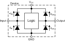
GUID-D7325FB5-82DB-463C-B1EB-F30785061834-low.gifFigure 8-1 Electrical Placement of Clamping Diodes for Each Input and Output