ZHCSPD1D February 1998 – November 2021 CD54HC165 , CD54HCT165 , CD74HC165 , CD74HCT165
PRODUCTION DATA
6 Parameter Measurement Information
Phase relationships between waveforms were chosen arbitrarily. All input pulses are supplied by generators having the following characteristics: PRR ≤ 1 MHz, ZO = 50 Ω, tt < 6 ns.
For clock inputs, fmax is measured when the input duty cycle is 50%.
The outputs are measured one at a time with one input transition per measurement.
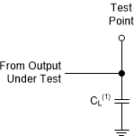
(1) CL includes probe
and test-fixture capacitance.
Figure 6-1 Load Circuit for Push-Pull
Outputs Figure 6-2 Voltage Waveforms,
Standard CMOS Inputs Pulse Duration
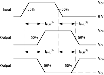
(1) The
greater between tPLH and tPHL is the same as
tpd.
Figure 6-4 Voltage Waveforms,
Standard CMOS Inputs Setup Propagation Delays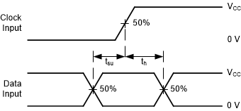 Figure 6-3 Voltage Waveforms,
Standard CMOS Inputs Setup and Hold Times
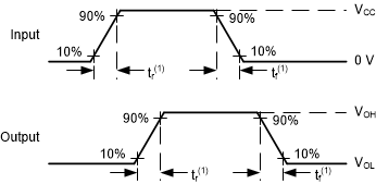
(1) The greater between
tr and tf is the same as tt.
Figure 6-5 Voltage Waveforms, Input
and Output Transition Times for Standard CMOS Input Devices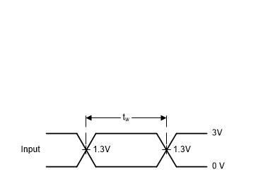 Figure 6-6 Voltage Waveforms,
TTL-Compatible CMOS Inputs Pulse Duration
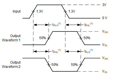
(1) The greater between
tPLH and tPHL is the same as
tpd.
Figure 6-8 Voltage Waveforms,
TTL-Compatible CMOS Inputs Propagation Delays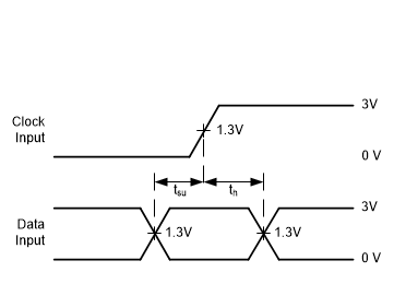 Figure 6-7 Voltage Waveforms,
TTL-Compatible CMOS Inputs Setup and Hold Times