ZHCSWV5C January 2001 – August 2024 CD54ACT00 , CD74ACT00
PRODUCTION DATA
- 1
- 1 特性
- 2 说明
- 3 Pin Configuration and Functions
- 4 Specifications
- 5 Parameter Measurement Information
- 6 Detailed Description
- 7 Application and Implementation
- 8 Device and Documentation Support
- 9 Revision History
- 10Mechanical, Packaging, and Orderable Information
封装选项
请参考 PDF 数据表获取器件具体的封装图。
机械数据 (封装 | 引脚)
- D|14
- N|14
散热焊盘机械数据 (封装 | 引脚)
订购信息
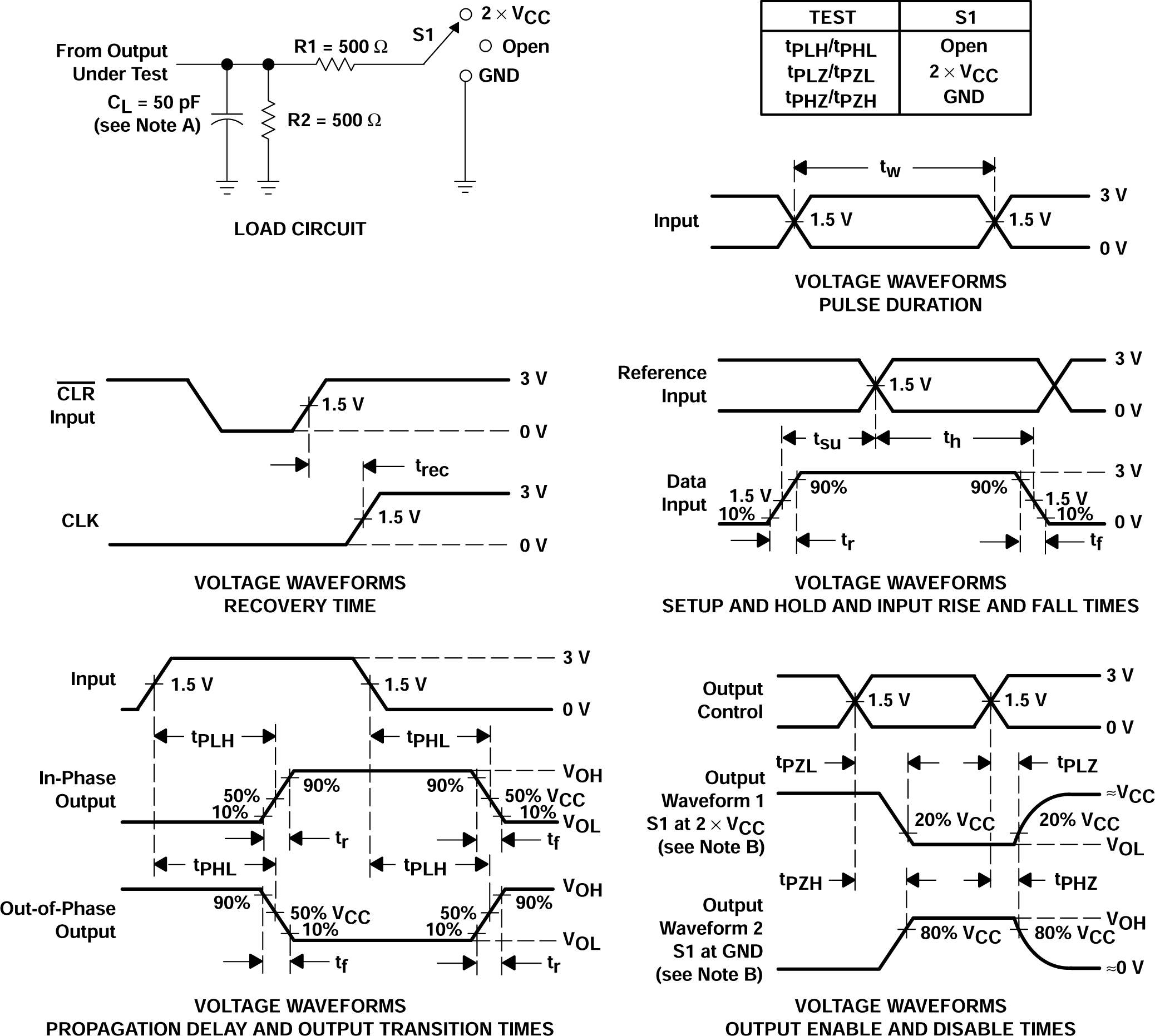
5 Parameter Measurement Information

A. CL includes probe and test-fixture capacitance.
B. Waveform 1 is for an output with internal conditions such that the output is low except when disabled by the output control. Waveform 2 is for an output with internal conditions such that the output is high except when disabled by the output control.
C. All input pulses are supplied by generators having the following characteristics: PRR ≤ 1 MHz, ZO = 50 Ω, tr = 3 ns, tf = 3 ns. Phase relationships between waveforms are arbitrary.
D. For clock inputs, fmax is measured with the input duty cycle at 50%.
E. The outputs are measured one at a time with one input transition per measurement.
F. tPLH and tPHL are the same as tpd.
G. tPZL and tPZH are the same as ten.
H. tPLZ and tPHZ are the same as tdis.
Figure 5-1 Load Circuit and Voltage Waveforms