ZHCSRI9F August   1997  – April 2021 CD54HC11 , CD74HC11

PRODUCTION DATA  

  1. 特性
  2. 应用
  3. 说明
  4. Revision History
    1.     5
      1.      Pin Functions
  5. Specifications
    1. 5.1 Absolute Maximum Ratings
    2. 5.2 ESD Ratings
    3. 5.3 Recommended Operating Conditions
    4. 5.4 Thermal Information
    5. 5.5 Electrical Characteristics
    6. 5.6 Switching Characteristics
    7. 5.7 Operating Characteristics
    8. 5.8 Typical Characteristics
  6. Parameter Measurement Information
  7. Detailed Description
    1. 7.1 Overview
    2. 7.2 Functional Block Diagram
    3. 7.3 Feature Description
      1. 7.3.1 Balanced CMOS Push-Pull Outputs
      2. 7.3.2 Standard CMOS Inputs
      3. 7.3.3 Clamp Diode Structure
    4. 7.4 Device Functional Modes
  8. Application and Implementation
    1. 8.1 Application Information
    2. 8.2 Typical Application
      1. 8.2.1 Design Requirements
        1. 8.2.1.1 Power Considerations
        2. 8.2.1.2 Input Considerations
        3. 8.2.1.3 Output Considerations
      2. 8.2.2 Detailed Design Procedure
      3. 8.2.3 Application Curves
        1.       Power Supply Recommendations
  9. Layout
    1. 9.1 Layout Guidelines
    2. 9.2 Layout Example
  10. 10Device and Documentation Support
    1. 10.1 Documentation Support
      1. 10.1.1 Related Documentation
    2. 10.2 接收文档更新通知
    3. 10.3 支持资源
    4. 10.4 Trademarks
    5. 10.5 静电放电警告
    6. 10.6 Related Links
    7. 10.7 Community Resources
    8. 10.8 术语表
      1.      Mechanical, Packaging, and Orderable Information

封装选项

请参考 PDF 数据表获取器件具体的封装图。

机械数据 (封装 | 引脚)
  • D|14
  • N|14
散热焊盘机械数据 (封装 | 引脚)
订购信息

Parameter Measurement Information

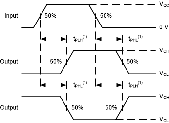
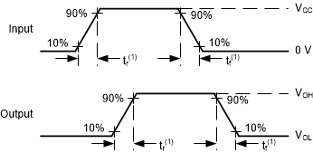
  • Phase relationships between waveforms were chosen arbitrarily. All input pulses are supplied by generators having the following characteristics: PRR ≤ 1 MHz, ZO = 50 Ω, tt < 6 ns.
  • The outputs are measured one at a time, with one input transition per measurement.
GUID-2246B453-FD36-408D-8C4C-3D05AF478B0C-low.gif
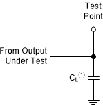
CL= 50 pF and includes probe and jig capacitance.
Figure 6-1 Load Circuit
GUID-CF0C1767-7413-4A47-8536-3B8F5D3C5DA1-low.gif
The maximum between tPLH and tPHL is used for tpd.
Figure 6-3 Voltage Waveforms Propagation Delays
GUID-38204D79-8ABA-402E-A2B7-553109AC2FA7-low.gif
tt is the greater of tr and tf.
Figure 6-2 Voltage Waveforms Transition Times