ZHCSKG8B November   2019  – October 2024 CDCDB2000

PRODUCTION DATA  

  1.   1
  2. 特性
  3. 应用
  4. 说明
  5. Pin Configuration and Functions
  6. Specifications
    1. 5.1 Absolute Maximum Ratings
    2. 5.2 ESD Ratings
    3. 5.3 Recommended Operating Conditions
    4. 5.4 Thermal Information
    5. 5.5 Electrical Characteristics
    6. 5.6 Timing Requirements
    7. 5.7 Typical Characteristics
  7. Detailed Description
    1. 6.1 Overview
    2. 6.2 Functional Block Diagram
    3. 6.3 Feature Description
      1. 6.3.1 Output Enable Control
      2. 6.3.2 SMBus
        1. 6.3.2.1 SMBus Address Assignment
      3. 6.3.3 Side-Band Interface
    4. 6.4 Device Functional Modes
      1. 6.4.1 CKPWRGD_PD# Function
      2. 6.4.2 OE[12:5]# and SMBus Output Enables
    5. 6.5 Programming
      1. 6.5.1 SMBus
      2. 6.5.2 SBI
  8. Register Maps
    1. 7.1 CDCDB2000 Registers
  9. Application and Implementation
    1. 8.1 Application Information
    2. 8.2 Typical Application
      1. 8.2.1 Design Requirements
      2. 8.2.2 Detailed Design Procedure
        1. 8.2.2.1 Output Enable Control Method
        2. 8.2.2.2 SMBus Address
      3. 8.2.3 Application Curve
    3. 8.3 Power Supply Recommendations
    4. 8.4 Layout
      1. 8.4.1 Layout Guidelines
      2. 8.4.2 Layout Examples
  10. Device and Documentation Support
    1. 9.1 Device Support
      1. 9.1.1 TICS Pro
    2. 9.2 接收文档更新通知
    3. 9.3 支持资源
    4. 9.4 Trademarks
    5. 9.5 静电放电警告
    6. 9.6 术语表
  11. 10Revision History
  12. 11Mechanical, Packaging, and Orderable Information

封装选项

机械数据 (封装 | 引脚)
散热焊盘机械数据 (封装 | 引脚)
订购信息

Programming

The CDCDB2000 has two methods to program the states of its 20 output drivers: SMBus and SBI.

To select between SMBus and SBI interfaces, the SBEN pin is used. Pulling the SBEN to a high level enables the SBI. Pulling the SBEN pin to ground enables the SMBus interface. When SBI is enabled, the SMBus Mask registers are active. The SMBus Mask registers allow the function of the SBI shift registers to be disabled and set the each individual channel as enabled. See Figure 6-2 for a diagram of how the SMBus Mask registers and SBI shift register interact to enable or disable each output.
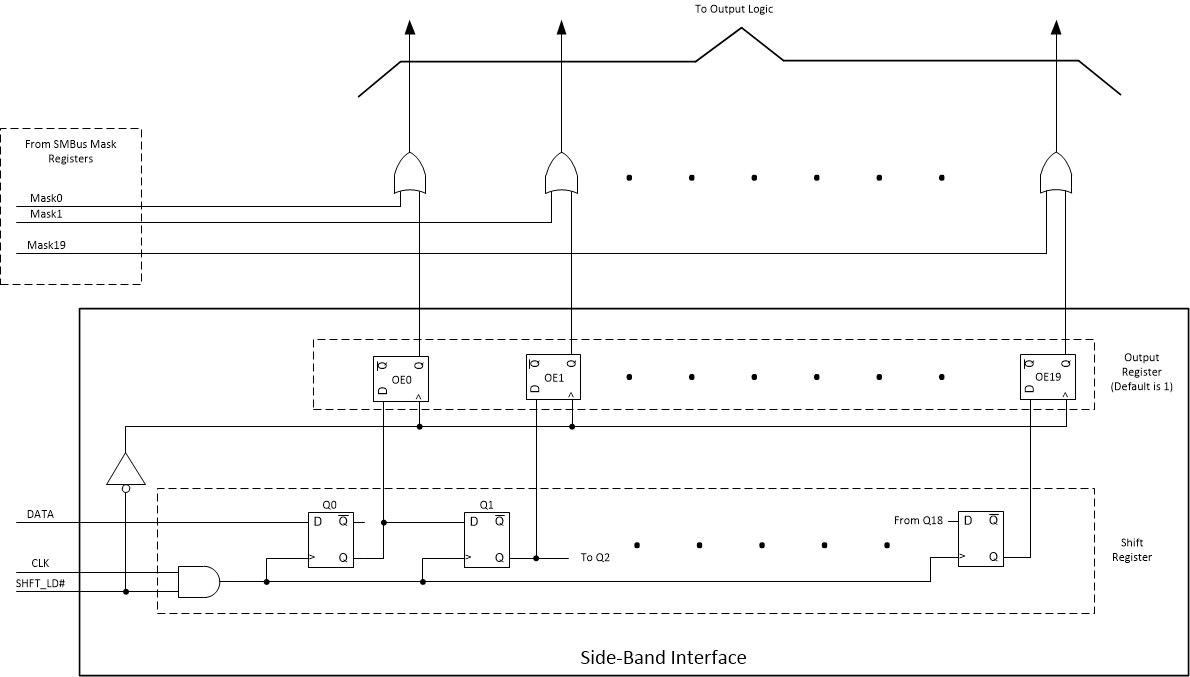
CDCDB2000 SMBus
                    Mask Register and SBI Shift Register Logic Figure 6-2 SMBus Mask Register and SBI Shift Register Logic