ZHCSKG8B November   2019  – October 2024 CDCDB2000

PRODUCTION DATA  

  1.   1
  2. 特性
  3. 应用
  4. 说明
  5. Pin Configuration and Functions
  6. Specifications
    1. 5.1 Absolute Maximum Ratings
    2. 5.2 ESD Ratings
    3. 5.3 Recommended Operating Conditions
    4. 5.4 Thermal Information
    5. 5.5 Electrical Characteristics
    6. 5.6 Timing Requirements
    7. 5.7 Typical Characteristics
  7. Detailed Description
    1. 6.1 Overview
    2. 6.2 Functional Block Diagram
    3. 6.3 Feature Description
      1. 6.3.1 Output Enable Control
      2. 6.3.2 SMBus
        1. 6.3.2.1 SMBus Address Assignment
      3. 6.3.3 Side-Band Interface
    4. 6.4 Device Functional Modes
      1. 6.4.1 CKPWRGD_PD# Function
      2. 6.4.2 OE[12:5]# and SMBus Output Enables
    5. 6.5 Programming
      1. 6.5.1 SMBus
      2. 6.5.2 SBI
  8. Register Maps
    1. 7.1 CDCDB2000 Registers
  9. Application and Implementation
    1. 8.1 Application Information
    2. 8.2 Typical Application
      1. 8.2.1 Design Requirements
      2. 8.2.2 Detailed Design Procedure
        1. 8.2.2.1 Output Enable Control Method
        2. 8.2.2.2 SMBus Address
      3. 8.2.3 Application Curve
    3. 8.3 Power Supply Recommendations
    4. 8.4 Layout
      1. 8.4.1 Layout Guidelines
      2. 8.4.2 Layout Examples
  10. Device and Documentation Support
    1. 9.1 Device Support
      1. 9.1.1 TICS Pro
    2. 9.2 接收文档更新通知
    3. 9.3 支持资源
    4. 9.4 Trademarks
    5. 9.5 静电放电警告
    6. 9.6 术语表
  11. 10Revision History
  12. 11Mechanical, Packaging, and Orderable Information

封装选项

机械数据 (封装 | 引脚)
散热焊盘机械数据 (封装 | 引脚)
订购信息

Layout Examples

Figure 8-3 and Figure 8-4 are PCB layout examples that show the application of thermal design practices and a low-inductance ground connection between the device DAP and the PCB.

The CDCDB2000 has 85-Ω differential output impedance LP-HCSL format drivers. All transmission lines connected to CKx pins should be 85-Ω differential impedance, 42.5-Ω single-ended impedance to avoid reflections and increased radiated emissions. Take care to eliminate or reduce stubs on the transmission lines.
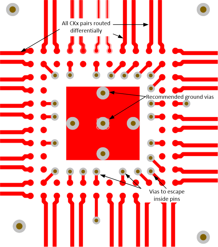
CDCDB2000 PCB Layout Example for CDCDB2000, Top LayerFigure 8-3 PCB Layout Example for CDCDB2000, Top Layer
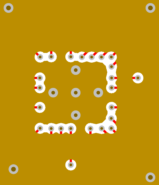
CDCDB2000 PCB Layout Example for CDCDB2000, GND LayerFigure 8-4 PCB Layout Example for CDCDB2000, GND Layer
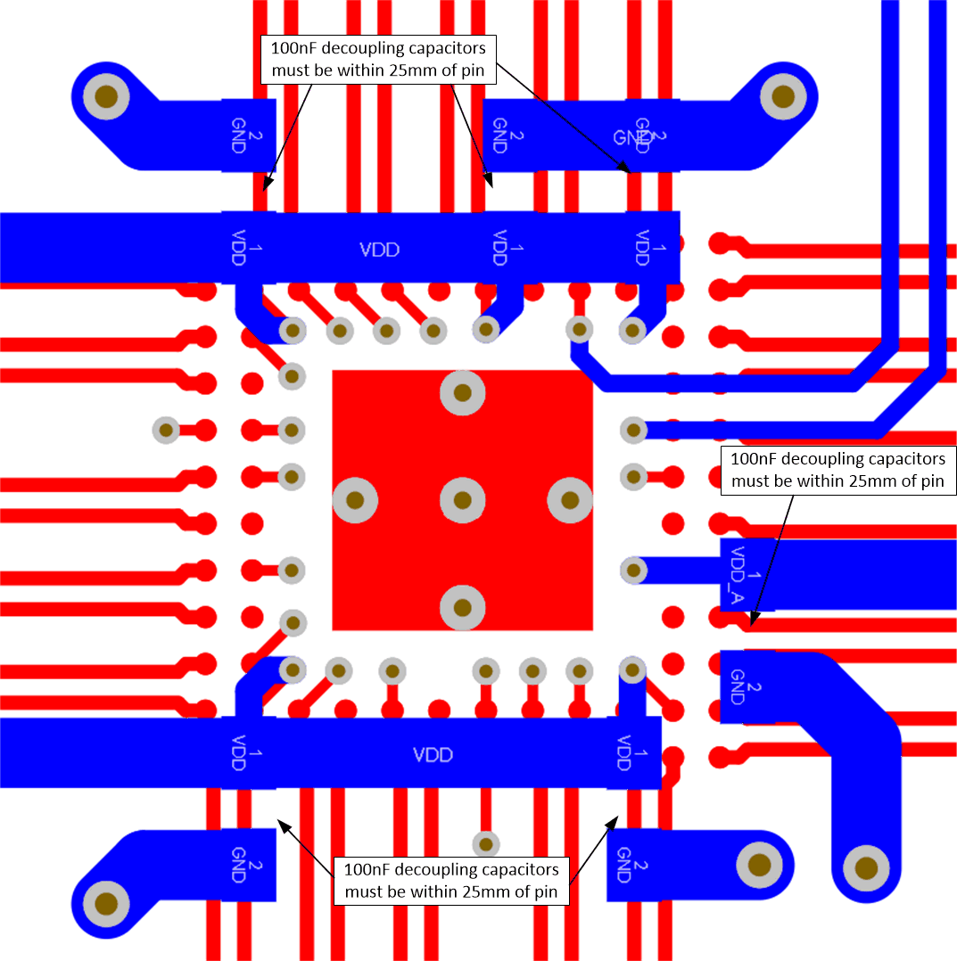
CDCDB2000 PCB Layout Example for CDCDB2000, Bottom LayerFigure 8-5 PCB Layout Example for CDCDB2000, Bottom Layer