ZHCSKG8B November   2019  – October 2024 CDCDB2000

PRODUCTION DATA  

  1.   1
  2. 特性
  3. 应用
  4. 说明
  5. Pin Configuration and Functions
  6. Specifications
    1. 5.1 Absolute Maximum Ratings
    2. 5.2 ESD Ratings
    3. 5.3 Recommended Operating Conditions
    4. 5.4 Thermal Information
    5. 5.5 Electrical Characteristics
    6. 5.6 Timing Requirements
    7. 5.7 Typical Characteristics
  7. Detailed Description
    1. 6.1 Overview
    2. 6.2 Functional Block Diagram
    3. 6.3 Feature Description
      1. 6.3.1 Output Enable Control
      2. 6.3.2 SMBus
        1. 6.3.2.1 SMBus Address Assignment
      3. 6.3.3 Side-Band Interface
    4. 6.4 Device Functional Modes
      1. 6.4.1 CKPWRGD_PD# Function
      2. 6.4.2 OE[12:5]# and SMBus Output Enables
    5. 6.5 Programming
      1. 6.5.1 SMBus
      2. 6.5.2 SBI
  8. Register Maps
    1. 7.1 CDCDB2000 Registers
  9. Application and Implementation
    1. 8.1 Application Information
    2. 8.2 Typical Application
      1. 8.2.1 Design Requirements
      2. 8.2.2 Detailed Design Procedure
        1. 8.2.2.1 Output Enable Control Method
        2. 8.2.2.2 SMBus Address
      3. 8.2.3 Application Curve
    3. 8.3 Power Supply Recommendations
    4. 8.4 Layout
      1. 8.4.1 Layout Guidelines
      2. 8.4.2 Layout Examples
  10. Device and Documentation Support
    1. 9.1 Device Support
      1. 9.1.1 TICS Pro
    2. 9.2 接收文档更新通知
    3. 9.3 支持资源
    4. 9.4 Trademarks
    5. 9.5 静电放电警告
    6. 9.6 术语表
  11. 10Revision History
  12. 11Mechanical, Packaging, and Orderable Information

封装选项

机械数据 (封装 | 引脚)
散热焊盘机械数据 (封装 | 引脚)
订购信息

CKPWRGD_PD# Function

The CKPWRGD_PD# pin is used to set 2 state variables inside of the device: PWRGD, and PD#. The PWRGD and PD# variables control which functions of the device are active at any time, as well as the state of the input and output pins.

The PWRGD and PD# states are multiplexed on the CKPWRGD_PD# pin. CKPWRGD_PD# must remain below VOL and not exceed VDD_A + 0.3 V until VDD, VDD_A, and CLKIN are present and within the recommended operating conditions.

The first rising edge of the CKPWRGD_PD# pin sets PWRGD = 1. After PWRGD is set to 1, the CKPWRGD_PD# pin is used to assert PD# mode only. PWRGD variable will only be cleared to 0 with the removal of VDD and VDD_A.
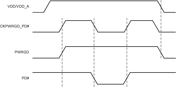
CDCDB2000 PWRGD and PD# State ChangesFigure 6-1 PWRGD and PD# State Changes