ZHCSOD8A November   2021  – May 2022 CDCDB400

PRODUCTION DATA  

  1. 特性
  2. 应用
  3. 说明
  4. Revision History
  5. Pin Configuration and Functions
  6. Specifications
    1. 6.1 Absolute Maximum Ratings
    2. 6.2 ESD Ratings
    3. 6.3 Recommended Operating Conditions
    4. 6.4 Thermal Information
    5. 6.5 Electrical Characteristics
    6. 6.6 Timing Requirements
    7. 6.7 Typical Characteristics
  7. Parameter Measurement Information
  8. Detailed Description
    1. 8.1 Overview
    2. 8.2 Functional Block Diagram
    3. 8.3 Feature Description
      1. 8.3.1 Fail-Safe Input
      2. 8.3.2 Output Enable Control
      3. 8.3.3 SMBus
        1. 8.3.3.1 SMBus Address Assignment
    4. 8.4 Device Functional Modes
      1. 8.4.1 CKPWRGD_PD# Function
      2. 8.4.2 OE[3:0]# and SMBus Output Enables
      3. 8.4.3 Output Slew Rate Control
      4. 8.4.4 Output Impedance Control
    5. 8.5 Programming
    6. 8.6 Register Maps
      1. 8.6.1 CDCDB400 Registers
  9. Application and Implementation
    1. 9.1 Application Information
    2. 9.2 Typical Application
      1. 9.2.1 Design Requirements
      2. 9.2.2 Detailed Design Procedure
        1. 9.2.2.1 Output Enable Control Method
        2. 9.2.2.2 SMBus Address
      3. 9.2.3 Application Curves
  10. 10Power Supply Recommendations
  11. 11Layout
    1. 11.1 Layout Guidelines
    2. 11.2 Layout Examples
  12. 12Device and Documentation Support
    1. 12.1 Device Support
      1. 12.1.1 TICS Pro
    2. 12.2 接收文档更新通知
    3. 12.3 支持资源
    4. 12.4 Trademarks
    5. 12.5 Electrostatic Discharge Caution
    6. 12.6 术语表
  13. 13Mechanical, Packaging, and Orderable Information

封装选项

机械数据 (封装 | 引脚)
散热焊盘机械数据 (封装 | 引脚)
订购信息

Programming

The CDCDB400 uses SMBus to program the states of its four output drivers. See Section 8.3.3 for more information on the SMBus programming, and Section 8.6 for information on the registers.

Table 8-3 Command Code Definition
BITDESCRIPTION
70 = Block Read or Block Write operation
1 = Byte Read or Byte Write operation
(6:0)Register address for Byte operations, or starting register address for Block, operations
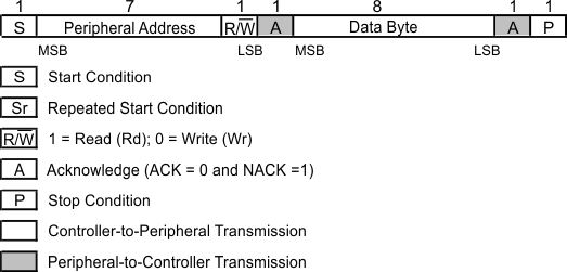
GUID-20210121-CA0I-LNZC-5KQQ-D4Q34XCF6DRT-low.gif Figure 8-2 Generic Programming Sequence
GUID-7F0F8034-F289-4BA7-AD76-7C1CE8538693-low.gifFigure 8-3 Byte Write Protocol
GUID-20210712-CA0I-XMSW-XFMQ-SR9CT8D6XNWN-low.gif Figure 8-4 Byte Read Protocol
GUID-3B27AD55-414A-4DCC-80D8-2A6D70009192-low.gifFigure 8-5 Block Write Protocol
GUID-20210712-CA0I-W1NM-SW7Z-NMN9ZWXXSJHR-low.gif Figure 8-6 Block Read Protocol
Figure 8-7 SMBus Timing Diagram