ZHCSOD8A November 2021 – May 2022 CDCDB400
PRODUCTION DATA
- 1 特性
- 2 应用
- 3 说明
- 4 Revision History
- 5 Pin Configuration and Functions
- 6 Specifications
- 7 Parameter Measurement Information
- 8 Detailed Description
- 9 Application and Implementation
- 10Power Supply Recommendations
- 11Layout
- 12Device and Documentation Support
- 13Mechanical, Packaging, and Orderable Information
11.2 Layout Examples
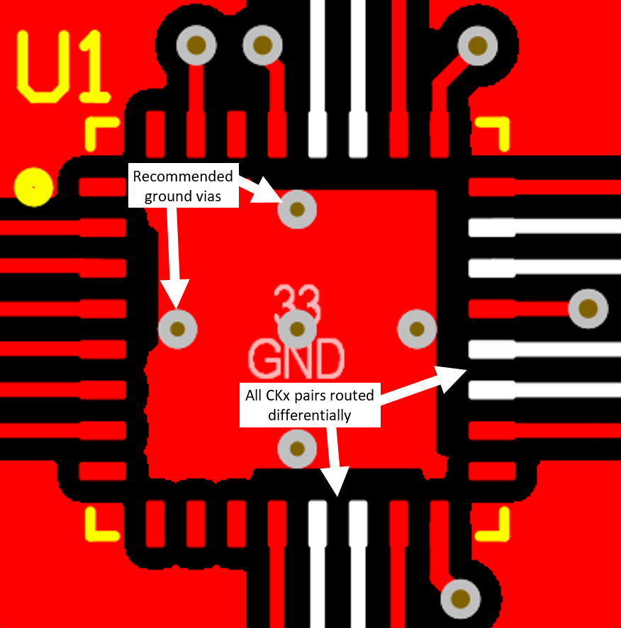
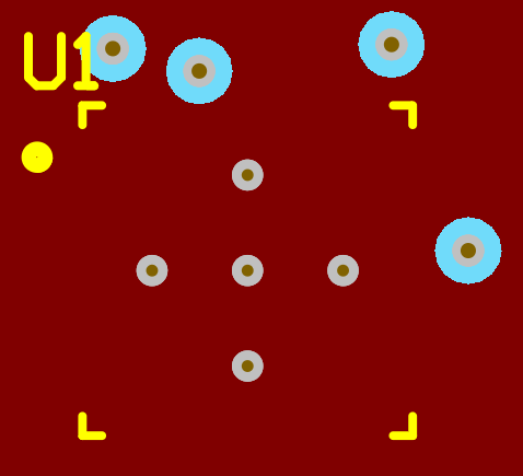
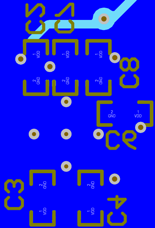
Figure 11-1 through Figure 11-3 are printed circuit board (PCB) layout examples that show the application of thermal design practices and a low-inductance ground connection between the device DAP and the PCB.
 Figure 11-1 PCB
Layout Example for CDCDB400, Top layer
 Figure 11-2 PCB
Layout Example for CDCDB400, GND Layer
 Figure 11-3 PCB
Layout Example for CDCDB400, Bottom Layer