ZHCSK34B July   2020  – October 2021 CDCE6214-Q1

PRODUCTION DATA  

  1. 特性
  2. 应用
  3. 说明
  4. Revision History
  5. 说明(续)
  6. Pin Configuration and Functions
  7. Specifications
    1. 7.1  Absolute Maximum Ratings
    2. 7.2  ESD Ratings
    3. 7.3  Recommended Operating Conditions
    4. 7.4  Thermal Information
    5. 7.5  EEPROM Characteristics
    6. 7.6  Reference Input, Single-Ended Characteristics
    7. 7.7  Reference Input, Differential Characteristics
    8. 7.8  Reference Input, Crystal Mode Characteristics
    9. 7.9  General-Purpose Input Characteristics
    10. 7.10 Triple Level Input Characteristics
    11. 7.11 Logic Output Characteristics
    12. 7.12 Phase Locked Loop Characteristics
    13. 7.13 Closed-Loop Output Jitter Characteristics
    14. 7.14 Input and Output Isolation
    15. 7.15 Buffer Mode Characteristics
    16. 7.16 PCIe Spread Spectrum Generator
    17. 7.17 LVCMOS Output Characteristics
    18. 7.18 LP-HCSL Output Characteristics
    19. 7.19 LVDS Output Characteristics
    20. 7.20 Output Synchronization Characteristics
    21. 7.21 Power-On Reset Characteristics
    22. 7.22 I2C-Compatible Serial Interface Characteristics
    23. 7.23 Timing Requirements, I2C-Compatible Serial Interface
    24. 7.24 Power Supply Characteristics
    25. 7.25 Typical Characteristics
  8. Parameter Measurement Information
    1. 8.1 Reference Inputs
    2. 8.2 Outputs
    3. 8.3 Serial Interface
    4. 8.4 PSNR Test
    5. 8.5 Clock Interfacing and Termination
      1. 8.5.1 Reference Input
      2. 8.5.2 Outputs
  9. Detailed Description
    1. 9.1 Overview
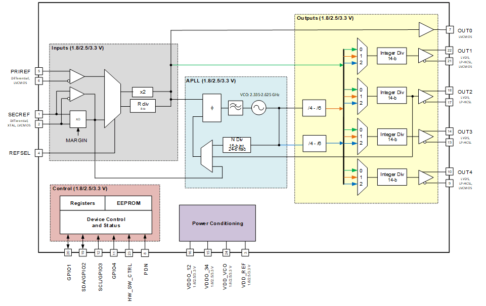
    2. 9.2 Functional Block Diagram
    3. 9.3 Feature Description
      1. 9.3.1 Reference Block
        1. 9.3.1.1 Zero Delay Mode, Internal and External Path
      2. 9.3.2 Phase-Locked Loop (PLL)
        1. 9.3.2.1 PLL Configuration and Divider Settings
        2. 9.3.2.2 Spread Spectrum Clocking
        3. 9.3.2.3 Digitally-Controlled Oscillator/ Frequency Increment and Decrement - Serial Interface Mode and GPIO Mode
      3. 9.3.3 Clock Distribution
        1. 9.3.3.1 Glitchless Operation
        2. 9.3.3.2 Divider Synchronization
        3. 9.3.3.3 Global and Individual Output Enable
      4. 9.3.4 Power Supplies and Power Management
      5. 9.3.5 Control Pins
    4. 9.4 Device Functional Modes
      1. 9.4.1 Operation Modes
        1. 9.4.1.1 Fall-Back Mode
        2. 9.4.1.2 Pin Mode
        3. 9.4.1.3 Serial Interface Mode
    5. 9.5 Programming
      1. 9.5.1 I2C Serial Interface
      2. 9.5.2 EEPROM
        1. 9.5.2.1 EEPROM - Cyclic Redundancy Check
        2. 9.5.2.2 Recommended Programming Procedure
        3. 9.5.2.3 EEPROM Access
          1. 9.5.2.3.1 Register Commit Flow
          2. 9.5.2.3.2 Direct Access Flow
        4. 9.5.2.4 Register Bits to EEPROM Mapping
  10. 10Application and Implementation
    1. 10.1 Application Information
    2. 10.2 Typical Application
      1. 10.2.1 Design Requirements
      2. 10.2.2 Detailed Design Procedure
      3. 10.2.3 Application Curves
  11. 11Power Supply Recommendations
    1. 11.1 Power-Up Sequence
    2. 11.2 Decoupling
  12. 12Layout
    1. 12.1 Layout Guidelines
    2. 12.2 Layout Examples
  13. 13Device and Documentation Support
    1. 13.1 Device Support
      1. 13.1.1 Development Support
      2. 13.1.2 Device Nomenclature
    2. 13.2 接收文档更新通知
    3. 13.3 支持资源
    4. 13.4 Trademarks
    5. 13.5 Electrostatic Discharge Caution
    6. 13.6 术语表
  14. 14Mechanical, Packaging, and Orderable Information

封装选项

请参考 PDF 数据表获取器件具体的封装图。

机械数据 (封装 | 引脚)
  • RGE|24
散热焊盘机械数据 (封装 | 引脚)
订购信息

Functional Block Diagram

GUID-EFDA4433-A730-4B9C-BA00-DCB39ECEE9A4-low.gifFigure 9-1 CDCE6214-Q1 Clock Generator With 2 Inputs, 1 Fractional-N PLL, and 4 Outputs