ZHCSK34B July 2020 – October 2021 CDCE6214-Q1
PRODUCTION DATA
- 1 特性
- 2 应用
- 3 说明
- 4 Revision History
- 5 说明(续)
- 6 Pin Configuration and Functions
-
7 Specifications
- 7.1 Absolute Maximum Ratings
- 7.2 ESD Ratings
- 7.3 Recommended Operating Conditions
- 7.4 Thermal Information
- 7.5 EEPROM Characteristics
- 7.6 Reference Input, Single-Ended Characteristics
- 7.7 Reference Input, Differential Characteristics
- 7.8 Reference Input, Crystal Mode Characteristics
- 7.9 General-Purpose Input Characteristics
- 7.10 Triple Level Input Characteristics
- 7.11 Logic Output Characteristics
- 7.12 Phase Locked Loop Characteristics
- 7.13 Closed-Loop Output Jitter Characteristics
- 7.14 Input and Output Isolation
- 7.15 Buffer Mode Characteristics
- 7.16 PCIe Spread Spectrum Generator
- 7.17 LVCMOS Output Characteristics
- 7.18 LP-HCSL Output Characteristics
- 7.19 LVDS Output Characteristics
- 7.20 Output Synchronization Characteristics
- 7.21 Power-On Reset Characteristics
- 7.22 I2C-Compatible Serial Interface Characteristics
- 7.23 Timing Requirements, I2C-Compatible Serial Interface
- 7.24 Power Supply Characteristics
- 7.25 Typical Characteristics
- 8 Parameter Measurement Information
- 9 Detailed Description
- 10Application and Implementation
- 11Power Supply Recommendations
- 12Layout
- 13Device and Documentation Support
- 14Mechanical, Packaging, and Orderable Information
9.3.3.2 Divider Synchronization
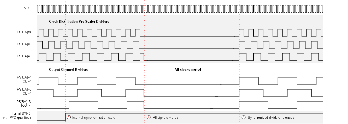
The output dividers can be reset in a deterministic way. This can be achieved using the sync bit or PDN pin. The level of the pin is qualified internally using the reference frequency at the PFD input. A low level on the SYNCN pin or sync bit will mute the outputs. A high level will synchronously release all output dividers to operation, so that all outputs share a common rising edge. The first rising edge can be individually delayed in steps of the respective pre-scalar period, up to 32 cycles using ch{x}_sync_delay. This allows the user to compensate external delays like routing mismatch, cables, or inherent delays introduced by logic gates in an FPGA design. Each channel can be included or excluded from the SYNC process. Divider synchronization can be enabled individually by ch{x}_sync_en.
For a deterministic behavior over power-cycles seen from input to output the reference divider must be set to 1. It should not divide the reference clock nor should the reference doubler be used.
 Figure 9-9 Output Divider Synchronization