SNAS811 July   2020  – May  CDCE6214

PRODUCTION DATA.  

  1. Features
  2. Applications
  3. Description
    1.     Application Example CDCE6214
  4. Revision History
  5. Description (cont.)
  6. Pin Configuration and Functions
    1.     Pin Functions G = Ground, P = Power I = Input, I/O = Input/Output, O = Output I, RPUPD = Input with Resistive Pull-up and Pull-down I, RPU = Input with Resistive Pull=up I/O, RPU = Input/Output with resistive pull-up
  7. Specifications
    1. 7.1  Absolute Maximum Ratings
    2. 7.2  ESD Ratings
    3. 7.3  Recommended Operating Conditions
    4. 7.4  Thermal Information
    5. 7.5  EEPROM Characteristics
    6. 7.6  Reference Input, Single-Ended Characteristics
    7. 7.7  Reference Input, Differential Characteristics
    8. 7.8  Reference Input, Crystal Mode Characteristics
    9. 7.9  General-Purpose Input Characteristics
    10. 7.10 Triple Level Input Characteristics
    11. 7.11 Logic Output Characteristics
    12. 7.12 Phase Locked Loop Characteristics
    13. 7.13 Closed-Loop Output Jitter Characteristics
    14. 7.14 Input and Output Isolation
    15. 7.15 Buffer Mode Characteristics
    16. 7.16 PCIe Spread Spectrum Generator
    17. 7.17 LVCMOS Output Characteristics
    18. 7.18 LP-HCSL Output Characteristics
    19. 7.19 LVDS Output Characteristics
    20. 7.20 Output Synchronization Characteristics
    21. 7.21 Power-On Reset Characteristics
    22. 7.22 I2C-Compatible Serial Interface Characteristics
    23. 7.23 Timing Requirements, I2C-Compatible Serial Interface
    24. 7.24 Power Supply Characteristics
    25. 7.25 Typical Characteristics
  8. Parameter Measurement Information
    1. 8.1 Reference Inputs
    2. 8.2 Outputs
    3. 8.3 Serial Interface
    4. 8.4 PSNR Test
    5. 8.5 Clock Interfacing and Termination
      1. 8.5.1 Reference Input
      2. 8.5.2 Outputs
  9. Detailed Description
    1. 9.1 Overview
    2. 9.2 Functional Block Diagram
    3. 9.3 Feature Description
      1. 9.3.1 Reference Block
        1. 9.3.1.1 Zero Delay Mode, Internal and External Path
      2. 9.3.2 Phase-Locked Loop (PLL)
        1. 9.3.2.1 PLL Configuration and Divider Settings
        2. 9.3.2.2 Spread Spectrum Clocking
        3. 9.3.2.3 Digitally-Controlled Oscillator/ Frequency Increment and Decrement - Serial Interface Mode and GPIO Mode
      3. 9.3.3 Clock Distribution
        1. 9.3.3.1 Glitchless Operation
        2. 9.3.3.2 Divider Synchronization
        3. 9.3.3.3 Global and Individual Output Enable
      4. 9.3.4 Power Supplies and Power Management
      5. 9.3.5 Control Pins
    4. 9.4 Device Functional Modes
      1. 9.4.1 Operation Modes
        1. 9.4.1.1 Fall-Back Mode
        2. 9.4.1.2 Pin Mode
        3. 9.4.1.3 Serial Interface Mode
    5. 9.5 Programming
      1. 9.5.1 I2C Serial Interface
      2. 9.5.2 EEPROM
        1. 9.5.2.1 EEPROM - Cyclic Redundancy Check
        2. 9.5.2.2 Recommended Programming Procedure
        3. 9.5.2.3 EEPROM Access
          1. 9.5.2.3.1 Register Commit Flow
          2. 9.5.2.3.2 Direct Access Flow
        4. 9.5.2.4 Register Bits to EEPROM Mapping
  10. 10Application and Implementation
    1. 10.1 Application Information
    2. 10.2 Typical Application
      1. 10.2.1 Design Requirements
      2. 10.2.2 Detailed Design Procedure
      3. 10.2.3 Application Curves
  11. 11Power Supply Recommendations
    1. 11.1 Power-Up Sequence
    2. 11.2 Decoupling
  12. 12Layout
    1. 12.1 Layout Guidelines
    2. 12.2 Layout Examples
  13. 13Device and Documentation Support
    1. 13.1 Device Support
      1. 13.1.1 Development Support
      2. 13.1.2 Device Nomenclature
    2. 13.2 Receiving Notification of Documentation Updates
    3. 13.3 Support Resources
    4. 13.4 Trademarks
    5. 13.5 Electrostatic Discharge Caution
    6. 13.6 Glossary
  14. 14Mechanical, Packaging, and Orderable Information

封装选项

机械数据 (封装 | 引脚)
散热焊盘机械数据 (封装 | 引脚)
订购信息

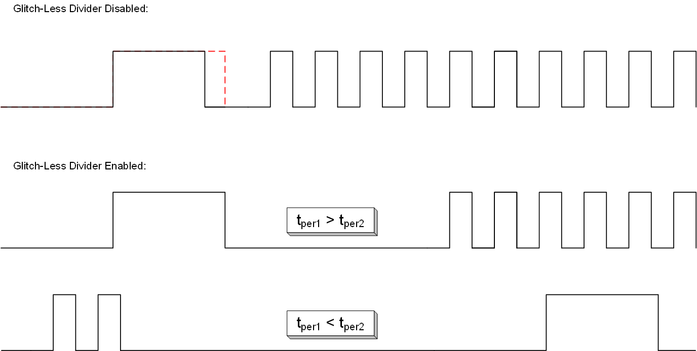
Glitchless Operation

The bit fields ch{x}_glitchless_en can be used to enable glitchless output divider update. This feature ensures that the high pulse of a clock period is not cut off by the output divider update process. It also ensures that setup and hold time of a receiver is not violated. The low pulse in the transition from earlier period to the new period is extended accordingly.
CDCE6214 timdiag_glitchless.gifFigure 30. Glitchless Divider Update