SNAS811
July 2020 – May
CDCE6214
PRODUCTION DATA.
1
Features
2
Applications
3
Description
Application Example CDCE6214
4
Revision History
5
Description (cont.)
6
Pin Configuration and Functions
Pin Functions G = Ground, P = Power I = Input, I/O = Input/Output, O = Output I, RPUPD = Input with Resistive Pull-up and Pull-down I, RPU = Input with Resistive Pull=up I/O, RPU = Input/Output with resistive pull-up
7
Specifications
7.1
Absolute Maximum Ratings
7.2
ESD Ratings
7.3
Recommended Operating Conditions
7.4
Thermal Information
7.5
EEPROM Characteristics
7.6
Reference Input, Single-Ended Characteristics
7.7
Reference Input, Differential Characteristics
7.8
Reference Input, Crystal Mode Characteristics
7.9
General-Purpose Input Characteristics
7.10
Triple Level Input Characteristics
7.11
Logic Output Characteristics
7.12
Phase Locked Loop Characteristics
7.13
Closed-Loop Output Jitter Characteristics
7.14
Input and Output Isolation
7.15
Buffer Mode Characteristics
7.16
PCIe Spread Spectrum Generator
7.17
LVCMOS Output Characteristics
7.18
LP-HCSL Output Characteristics
7.19
LVDS Output Characteristics
7.20
Output Synchronization Characteristics
7.21
Power-On Reset Characteristics
7.22
I2C-Compatible Serial Interface Characteristics
7.23
Timing Requirements, I2C-Compatible Serial Interface
7.24
Power Supply Characteristics
7.25
Typical Characteristics
8
Parameter Measurement Information
8.1
Reference Inputs
8.2
Outputs
8.3
Serial Interface
8.4
PSNR Test
8.5
Clock Interfacing and Termination
8.5.1
Reference Input
8.5.2
Outputs
9
Detailed Description
9.1
Overview
9.2
Functional Block Diagram
9.3
Feature Description
9.3.1
Reference Block
9.3.1.1
Zero Delay Mode, Internal and External Path
9.3.2
Phase-Locked Loop (PLL)
9.3.2.1
PLL Configuration and Divider Settings
9.3.2.2
Spread Spectrum Clocking
9.3.2.3
Digitally-Controlled Oscillator/ Frequency Increment and Decrement - Serial Interface Mode and GPIO Mode
9.3.3
Clock Distribution
9.3.3.1
Glitchless Operation
9.3.3.2
Divider Synchronization
9.3.3.3
Global and Individual Output Enable
9.3.4
Power Supplies and Power Management
9.3.5
Control Pins
9.4
Device Functional Modes
9.4.1
Operation Modes
9.4.1.1
Fall-Back Mode
9.4.1.2
Pin Mode
9.4.1.3
Serial Interface Mode
9.5
Programming
9.5.1
I2C Serial Interface
9.5.2
EEPROM
9.5.2.1
EEPROM - Cyclic Redundancy Check
9.5.2.2
Recommended Programming Procedure
9.5.2.3
EEPROM Access
9.5.2.3.1
Register Commit Flow
9.5.2.3.2
Direct Access Flow
9.5.2.4
Register Bits to EEPROM Mapping
10
Application and Implementation
10.1
Application Information
10.2
Typical Application
10.2.1
Design Requirements
10.2.2
Detailed Design Procedure
10.2.3
Application Curves
11
Power Supply Recommendations
11.1
Power-Up Sequence
11.2
Decoupling
12
Layout
12.1
Layout Guidelines
12.2
Layout Examples
13
Device and Documentation Support
13.1
Device Support
13.1.1
Development Support
13.1.2
Device Nomenclature
13.2
Receiving Notification of Documentation Updates
13.3
Support Resources
13.4
Trademarks
13.5
Electrostatic Discharge Caution
13.6
Glossary
14
Mechanical, Packaging, and Orderable Information
封装选项
机械数据 (封装 | 引脚)
RGE|24
MPQF124G
散热焊盘机械数据 (封装 | 引脚)
RGE|24
QFND593
订购信息
snas811_oa
snas811_pm
8.5.2
Outputs
Figure 19.
LVCMOS Output
Figure 20.
LVDS Output - DC-Coupled. Place 100Ω close to the DUT
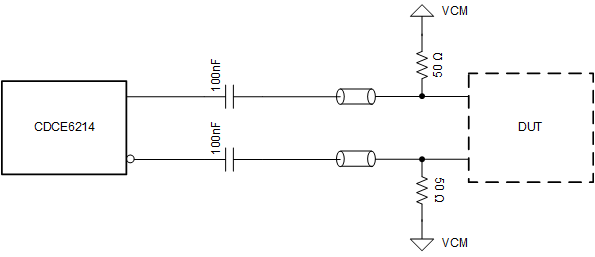
Figure 21.
LVDS Output - AC-Coupled
Figure 22.
LP-HCSL Output
千亿体育app官网登录(中国)官方网站IOS/安卓通用版/手机APP
|
米乐app下载官网(中国)|ios|Android/通用版APP最新版
|
米乐|米乐·M6(中国大陆)官方网站
|
千亿体育登陆地址
|
华体会体育(中国)HTH·官方网站
|
千赢qy国际_全站最新版千赢qy国际V6.2.14安卓/IOS下载
|
18新利网v1.2.5|中国官方网站
|
bob电竞真人(中国官网)安卓/ios苹果/电脑版【1.97.95版下载】
|
千亿体育app官方下载(中国)官方网站IOS/安卓/手机APP下载安装
|