ZHCSEA7A June 2015 – September 2015 CDCEL824
PRODUCTION DATA.
- 1 特性
- 2 应用
- 3 说明
- 4 修订历史记录
- 5 说明(续)
- 6 Pin Configuration and Functions
- 7 Specifications
- 8 Parameter Measurement Information
- 9 Detailed Description
- 10Application and Implementation
- 11Power Supply Recommendations
- 12Layout
- 13器件和文档支持
- 14机械、封装和可订购信息
9 Detailed Description
9.1 Overview
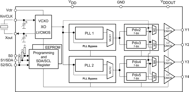
The CDCEL824 is a modular PLL-based low-cost, high-performance, programmable clock synthesizer, multiplier, and divider. It generates up to four output clocks from a single input frequency. Each output can be programmed in-system for any clock frequency up to 201 MHz, using up to two independent configurable PLLs.
The CDCEL824 has a separate output supply pins, VDDOUT, which are 1.8 V.
The input accepts an external crystal or LVCMOS clock signal. In case of a crystal input, an on-chip load capacitor is adequate for most applications. The value of the load capacitor is programmable from 0 pF to 20 pF.
The deep M/N divider ratio allows the generation of zero-ppm audio/video, networking (WLAN, Bluetooth, Ethernet, GPS) or interface (USB, IEEE1394, memory stick) clocks from a 27-MHz reference input frequency, for example.
Based on the PLL frequency and the divider settings, the internal loop filter components are automatically adjusted to achieve high stability and optimized jitter transfer characteristic of each PLL.
The device supports nonvolatile EEPROM programming for easy customization of the device in the application. It is preset to a factory default configuration and can be reprogrammed to a different application configuration before it goes onto the PCB or reprogrammed by in-system programming. All device settings are programmable through the SDA/SCL bus, a 2-wire serial interface.
Three, free programmable control inputs, S0, S1, and S2, can be used to select different frequencies, or other control features like outputs disable to low, outputs in high-impedance state, power down, PLL bypass, and so forth.
The CDCx824 operates in a 1.8-V environment. It operates in a temperature range of –40°C to 85°C.
9.2 Functional Block Diagram

9.3 Feature Description
9.3.1 Control Pins Settings
The CDCEL824 has three user-definable control pins (S0, S1, and S2) which allow external control of device settings. They can be programmed to any of the following settings:
- Frequency selection → switching between any of two user-defined frequencies
- Output state selection → output configuration and power-down control
The user can predefine up to eight different control settings. Table 1 and Table 2 explain these settings.
Table 1. Control Pin Definition
| EXTERNAL CONTROL BITS |
PLL1 SETTING | PLL2 SETTING | RSVD SETTING | ||||
|---|---|---|---|---|---|---|---|
| Control function | PLL frequency selection | Reserved | Output Y1/Y2 selection | PLL frequency selection | Reserved | Output Y3/Y4 selection | Reserved |
Table 2. PLL Setting (Can Be Selected for Each PLL Individual)(1)
| FREQUENCY SELECTION(2) | ||||
|---|---|---|---|---|
| FSx | FUNCTION | |||
| 0 | Frequency0 | |||
| 1 | Frequency1 | |||
| OUTPUT SELECTION(3) (Y1 ... Y4) | ||||
| YxYx | FUNCTION | |||
| 0 | State0 | |||
| 1 | State1 | |||
SDA/S1 and SCL/S2 pins of the CDCEL824 are dual-function pins. In the default configuration, they are predefined as the SDA/SCL serial programming interface. They can be programmed to control pins (S1/S2) by setting the relevant bits in the EEPROM. Note that the changes of the bits in the control register (bit [6] of byte 02h) have no effect until they are written into the EEPROM.
Once they are set as control pins, the serial programming interface is no longer available. However, if VDDOUT is forced to GND, the two control pins, S1 and S2, temporally act as serial programming pins (SDA/SCL).
S0 is not a multi-use pin; it is a control pin only.
9.3.2 SDA/SCL Serial Interface
This section describes the SDA/SCL interface of the CDCEL824 device. The CDCEL824 operates as a slave device of the 2-wire serial SDA/SCL bus, compatible with the popular SMBus or I2C specification. It operates in the standard-mode transfer (up to 100 kbit/s) and fast-mode transfer (up to 400 kbit/s) and supports 7-bit addressing.
The SDA/S1 and SCL/S2 pins of the CDCEL824 are dual-function pins. In the default configuration they are used as SDA/SCL serial programming interface. They can be reprogrammed as general-purpose control pins, S1 and S2, by changing the corresponding EEPROM setting, byte 02h, bit [6].
 Figure 5. Timing Diagram for SDA/SCL Serial Control Interface
9.3.3 SDA/SCL Hardware Interface
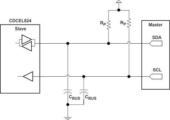
Figure 6 shows how the CDCEL824 clock synthesizer is connected to the SDA/SCL serial interface bus. Multiple devices can be connected to the bus, but the speed may need to be reduced (400 kHz is the maximum) if many devices are connected.
Note that the pullup resistors (RP) depend on the supply voltage, bus capacitance, and number of connected devices. The recommended pullup value is 4.7 kΩ. It must meet the minimum sink current of 3 mA at VOLmax = 0.4 V for the output stages (for more details see the SMBus or I2C Bus specification).
 Figure 6. SDA/SCL Hardware Interface
9.4 Device Functional Modes
9.4.1 Default Device Setting
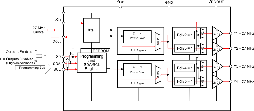
The internal EEPROM of CDCEL824 is preconfigured as shown in Figure 7. The input frequency is passed through the output as a default. This allows the device to operate in default mode without the extra production step of programming it. The default setting appears after power is supplied or after a power-down/up sequence until it is reprogrammed by the user to a different application configuration. A new register setting is programmed via the serial SDA/SCL interface.
 Figure 7. Preconfiguration of CDCEL824 Internal EEPROM
Table 3 shows the factory default setting for the control terminal register (external control pins). Note that even though eight different register settings are possible, in default configuration, only the first two settings (0 and 1) can be selected with S0, as S1 and S2 are configured as programming pins in the default mode.
Table 3. Factory Default Settings for Control Terminal Register(1)
| PLL1 SETTINGS | PLL2 SETTINGS | |||||
|---|---|---|---|---|---|---|
| EXTERNAL CONTROL PINS | FREQUENCY SELECTION | OUTPUT SELECTION | FREQUENCY SELECTION | OUTPUT SELECTION | ||
| S2 | S1 | S0 | FS1 | Y1Y2 | FS2 | Y2Y3 |
| SCL (I2C) | SDA (I2C) | 0 | fVCO1_0 | High-impedance state | fVCO2_0 | High-impedance state |
| SCL (I2C) | SDA (I2C) | 1 | fVCO1_0 | Enabled | fVCO2_0 | Enabled |
9.5 Programming
9.5.1 Data Protocol
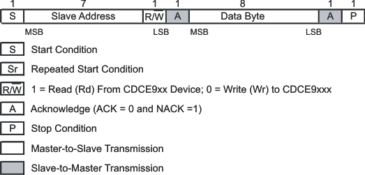
The device supports Byte Write and Byte Read and Block Write and Block Read operations.
For Byte Write/Read operations, the system controller can individually access addressed bytes.
For Block Write/Read operations, the bytes are accessed in sequential order from lowest to highest byte (with most-significant bit first) with the ability to stop after any complete byte has been transferred. The numbers of bytes read out are defined by byte count in the generic configuration register. At the Block Read instruction, all bytes defined in the byte count must be read out to finish the read cycle correctly.
Once a byte has been sent, it is written into the internal register and is effective immediately. This applies to each transferred byte regardless of whether this is a Byte Write or a Block Write sequence.
If the EEPROM write cycle is initiated, the internal SDA registers are written into the EEPROM. During this write cycle, data is not accepted at the SDA/SCL bus until the write cycle is completed. However, data can be read out during the programming sequence (Byte Read or Block Read). The programming status can be monitored by EEPIP, byte 01h–bit 6.
The offset of the indexed byte is encoded in the command code, as described in Table 4.
Table 4. Slave Receiver Address (7 Bits)
| DEVICE | A6 | A5 | A4 | A3 | A2 | A1(1) | A0(1) | R/W |
|---|---|---|---|---|---|---|---|---|
| CDCEL824 | 1 | 1 | 0 | 0 | 1 | 0 | 0 | 1/0 |
9.5.2 Command Code Definition
Table 5. Command Code Definition
| BIT | DESCRIPTION |
|---|---|
| 7 | 0 = Block Read or Block Write operation 1 = Byte Read or Byte Write operation |
| (6:0) | Byte offset for Byte Read, Block Read, Byte Write and Block Write operations. |
9.5.3 Generic Programming Sequence
 Figure 8. Generic Programming Sequence
9.5.4 Byte Write Programming Sequence
 Figure 9. Byte Write Protocol
9.5.6 Block Write Programming Sequence1

9.5.7 Block Read Programming Sequence
 Figure 12. Block Read Protocol
9.6 Register Maps
9.6.1 SDA/SCL Configuration Registers
The clock input, control pins, PLLs, and output stages are user configurable. The following tables and explanations describe the programmable functions of the CDCEL824. All settings can be manually written into the device via the SDA/SCL bus or easily programmed by using the TI Pro-Clock™ software.
Table 6. SDA/SCL Registers
| ADDRESS OFFSET | REGISTER DESCRIPTION | TABLE |
|---|---|---|
| 00h | Generic configuration register | Table 8 |
| 10h | PLL1 configuration register | Table 9 |
| 20h | PLL2 configuration register | Table 10 |
The grey-highlighted bits, described in the Configuration Registers tables in the following pages, belong to the Control Terminal Register. The user can predefine up to eight different control settings. These settings then can be selected by the external control pins, S0, S1, and S2. Table 7 explains the corresponding bit assignment between the Control Terminal Register and the Configuration Registers.
Table 7. Configuration Register, External Control Terminals
| PLL1 SETTINGS | PLL2 SETTINGS | ||||||
|---|---|---|---|---|---|---|---|
| EXTERNAL CONTROL PINS | FREQUENCY SELECTION |
OUTPUT SELECTION |
FREQUENCY SELECTION |
OUTPUT SELECTION |
|||
| S2 | S1 | S0 | FS1 | Y1Y2 | FS2 | Y3Y4 | |
| 0 | 0 | 0 | 0 | FS1_0 | Y1Y2_0 | FS2_0 | Y3Y4_0 |
| 1 | 0 | 0 | 1 | FS1_1 | Y1Y2_1 | FS2_1 | Y3Y4_1 |
| 2 | 0 | 1 | 0 | FS1_2 | Y1Y2_2 | FS2_2 | Y3Y4_2 |
| 3 | 0 | 1 | 1 | FS1_3 | Y1Y2_3 | FS2_3Reserved | Reserved |
| 4 | 1 | 0 | 0 | FS1_4 | Y1Y2_4 | FS2_4Reserved | Reserved |
| 5 | 1 | 0 | 1 | FS1_5 | Y1Y2_5 | FS2_5 | Y3Y4_5 |
| 6 | 1 | 1 | 0 | FS1_6 | Y1Y2_6 | FS2_6 | Y3Y4_6 |
| 7 | 1 | 1 | 1 | FS1_7 | Y1Y2_7 | FS2_7 | Y3Y4_7 |
| Address offset(1) | 13h | 15h | 23h | 25h | |||
Table 8. Generic Configuration Register
| OFFSET(1) | BIT(2) | ACRONYM | DEFAULT(3) | DESCRIPTION | ||||
|---|---|---|---|---|---|---|---|---|
| 00h | 7 | E_EL | 0b | Device identification (read-only): 0 is CDCEL824 (1.8 V out) | ||||
| 6:4 | RID | Xb | Revision identification number (read-only) | |||||
| 3:0 | VID | 1h | Vendor identification number (read-only) | |||||
| 01h | 7 | – | 0b | Reserved – always write 0 | ||||
| 6 | EEPIP | 0b | EEPROM programming Status4:(4) (read-only) | 0 – EEPROM programming is completed 1 – EEPROM is in programming mode |
||||
| 5 | EELOCK | 0b | Permanently lock EEPROM data(5) | 0 – EEPROM is not locked 1 – EEPROM is permanently locked |
||||
| 4 | PWDN | 0b | Device power down (overwrites S0/S1/S2 setting; configuration register settings are unchanged) Note: PWDN cannot be set to 1 in the EEPROM. 0 – Device active (all PLLs and all outputs are enabled) 1 – Device power down (all PLLs in power down and all outputs in high-impedance state) |
|||||
| 3:2 | INCLK | 00b | Input clock selection: | 00 – Xtal 01 – VCXO 10 – LVCMOS 1 – Reserved | ||||
| 1:0 | SLAVE_ADR | 00b | Address bits A0 and A1 of the slave receiver address | |||||
| 02h | 7 | M1 | 0b | RSVD | 0 – Input clock 1 – PLL1 clock | |||
| 6 | SPICON | 0b | Operation mode selection for pins 14/15(6)
0 – Serial programming interface SDA (pin 15) and SCL (pin 14) 1 – Control pins S1 (pin 15) and S2 (pin 14) |
|||||
| 5:4 | RSVD | 01b | RSVD | Reserved | ||||
| 3:2 | RSVD | 01b | ||||||
| 1:0 | RSVD | 001h | RSVD | Reserved | ||||
| 03h | 7:0 | RSVD | ||||||
| 04h | 7 | Reserved | 0b | RSVD | Reserved | |||
| 6 | Reserved | 0b | ||||||
| 5 | Reserved | 0b | ||||||
| 4 | Reserved | 0b | ||||||
| 3 | Reserved | 0b | ||||||
| 2 | Reserved | 0b | ||||||
| 1 | Reserved | 0b | ||||||
| 05h | 7:3 | XCSEL | 0Ah | Crystal load-capacitor selection(7) | 00h – 0 pF 01h – 1 pF 02h – 2 pF : 14h to 1Fh – 20 pF |
|||
| 2:0 | 0b | Reserved – do not write other than 0. | ||||||
| 06h | 7:1 | BCOUNT | 30h | 7-bit byte count (defines the number of bytes which will be sent from this device at the next Block Read transfer); all bytes must be read out to correctly finish the read cycle. | ||||
| 0 | EEWRITE | 0b | Initiate EEPROM write cycle(8) | 0 – No EEPROM write cycle 1 – Start EEPROM write cycle (internal registers are saved to the EEPROM) |
||||
| 07h-0Fh | — | 0h | Reserved – do not write other than 0 | |||||
Table 9. PLL1 Configuration Register
| OFFSET(1) | BIT(2) | ACRONYM | DEFAULT(3) | DESCRIPTION | |||
|---|---|---|---|---|---|---|---|
| 10h | 7:0 | Reserved | 00000000b | Reserved | |||
| 11h | 7:0 | Reserved | 00000000b | Reserved | |||
| 12h | 7:0 | Reserved | 00000000b | Reserved | |||
| 13h | 7 | FS1_7 | 0b | FS1_x: PLL1 frequency selection(4) | |||
| 6 | FS1_6 | 0b | 0 – fVCO1_0 (predefined by PLL1_0 – multiplier/divider value) 1 – fVCO1_1 (predefined by PLL1_1 – multiplier/divider value) |
||||
| 5 | FS1_5 | 0b | |||||
| 4 | FS1_4 | 0b | |||||
| 3 | FS1_3 | 0b | |||||
| 2 | FS1_2 | 0b | |||||
| 1 | FS1_1 | 0b | |||||
| 0 | FS1_0 | 0b | |||||
| 14h | 7 | MUX1 | 1b | PLL1 multiplexer: | 0 – PLL1 1 – PLL1 bypass (PLL1 is in power down) |
||
| 6 | M2 | 1b | Output Y1 multiplexer: | 0 – bypass 1 – Pdiv2 |
|||
| 5:4 | M3 | 10b | Output Y2 multiplexer: | 00 – bypass 01 – Pdiv2-divider 10 – Pdiv3-divider 11 – Reserved |
|||
| 3:2 | Y1Y2_ST1 | 11b | Y1, Y2-state0/1definition: | 00 – Y1/Y2 disabled to high-impedance state (PLL1 is in power down) 01 – Y1/Y2 disabled to high-impedance state (PLL1 on) 10 – Y1/Y2 disabled to low (PLL1 on) 11 – Y1/Y2 enabled (normal operation, PLL1 on) |
|||
| 1:0 | Y1Y2_ST0 | 01b | |||||
| 15h | 7 | Y1Y2_7 | 0b | Y1Y2_x output state selection(4) | |||
| 6 | Y1Y2_6 | 0b | 0 – state0 (predefined by Y1Y2_ST0) 1 – state1 (predefined by Y1Y2_ST1) |
||||
| 5 | Y1Y2_5 | 0b | |||||
| 4 | Y1Y2_4 | 0b | |||||
| 3 | Y1Y2_3 | 0b | |||||
| 2 | Y1Y2_2 | 0b | |||||
| 1 | Y1Y2_1 | 1b | |||||
| 0 | Y1Y2_0 | 0b | |||||
| 16h | 7 | Reserved | 0b | RSVD | Reserved | ||
| 6:0 | Pdiv2 | 01h | 7-bit Y1-output-divider Pdiv2: | 0 – Reset and in standby 1 to 127 – Divider value |
|||
| 17h | 7 | — | 0b | Reserved – do not write others than 0 | |||
| 6:0 | Pdiv3 | 01h | 7-bit Y2-output-divider Pdiv3: | 0 – Reset and in standby 1 to 127 – Divider value |
|||
| 18h | 7:0 | PLL1_0N [11:4 | 004h | PLL1_0(4): 30-bit multiplier/divider value for frequency fVCO1_0
(for more information, see the PLL Multiplier/Divider Definition paragraph). |
|||
| 19h | 7:4 | PLL1_0N [3:0] | |||||
| 3:0 | PLL1_0R [8:5] | 000h | |||||
| 1Ah | 7:3 | PLL1_0R[4:0] | |||||
| 2:0 | PLL1_0Q [5:3] | 10h | |||||
| 1Bh | 7:5 | PLL1_0Q [2:0] | |||||
| 4:2 | PLL1_0P [2:0] | 010b | |||||
| 1:0 | VCO1_0_RANGE | 00b | fVCO1_0 range selection: | 00 – fVCO1_0 < 125 MHz 01 – 125 MHz ≤ fVCO1_0 < 150 MHz 10 – 150 MHz ≤ fVCO1_0 < 175 MHz 11 – fVCO1_0 ≥ 175 MHz |
|||
| 1Ch | 7:0 | PLL1_1N [11:4] | 004h | PLL1_1(4): 30-bit multiplier/divider value for frequency fVCO1_1
(for more information see the PLL Multiplier/Divider Definition paragraph) |
|||
| 1Dh | 7:4 | PLL1_1N [3:0] | |||||
| 3:0 | PLL1_1R [8:5] | 000h | |||||
| 1Eh | 7:3 | PLL1_1R[4:0] | |||||
| 2:0 | PLL1_1Q [5:3] | 10h | |||||
| 1Fh | 7:5 | PLL1_1Q [2:0] | |||||
| 4:2 | PLL1_1P [2:0] | 010b | |||||
| 1:0 | VCO1_1_RANGE | 00b | fVCO1_1 range selection: | 00 – fVCO1_1 < 125 MHz 01 – 125 MHz ≤ fVCO1_1 < 150 MHz 10 – 150 MHz ≤ fVCO1_1 < 175 MHz 11 – fVCO1_1 ≥ 175 MHz |
|||
Table 10. PLL2 Configuration Register
| OFFSET(1) | BIT(2) | ACRONYM | DEFAULT(3) | DESCRIPTION | |||
|---|---|---|---|---|---|---|---|
| 20h | 7:0 | Reserved | 0000000b | Reserved | |||
| 21h | 7:0 | Reserved | 0000000b | Reserved | |||
| 22h | 7:0 | Reserved | 0000000b | Reserved | |||
| 23h | 7 | FS2_7 | 0b | FS2_x: PLL2 frequency selection(4) | |||
| 6 | FS2_6 | 0b | 0 – fVCO2_0 (predefined by PLL2_0 – multiplier/divider value) 1 – fVCO2_1 (predefined by PLL2_1 – multiplier/divider value) |
||||
| 5 | FS2_5 | 0b | |||||
| 4 | FS2_4 | 0b | |||||
| 3 | FS2_3 | 0b | |||||
| 2 | FS2_2 | 0b | |||||
| 1 | FS2_1 | 0b | |||||
| 0 | FS2_0 | 0b | |||||
| 24h | 7 | MUX2 | 1b | PLL2 multiplexer: | 0 – PLL2 1 – PLL2 bypass (PLL2 is in power down) |
||
| 6 | M4 | 1b | Output Y3 multiplexer: | 0 – Pdiv2 1 – Pdiv4 |
|||
| 5:4 | M5 | 10b | Output Y4 multiplexer: | 00 – Pdiv2-divider 01 – Pdiv4-divider 10 – Pdiv5-divider 11 – Reserved |
|||
| 3:2 | Y3Y4_ST1 | 11b | Y3, Y4-State0/1definition: | 00 – Y3/Y4 disabled to high-impedance state (PLL2 is in power down) 01 – Y3/Y4 disabled to high-impedance state (PLL2 on) 10–Y3/Y4 disabled to low (PLL2 on) 11 – Y3/Y4 enabled (normal operation, PLL2 on) |
|||
| 1:0 | Y3Y4_ST0 | 01b | |||||
| 25h | 7 | Y3Y4_7 | 0b | Y3Y4_x output state selection(4) | |||
| 6 | Y3Y4_6 | 0b | 0 – state0 (predefined by Y3Y4_ST0) 1 – state1 (predefined by Y3Y4_ST1) |
||||
| 5 | Y3Y4_5 | 0b | |||||
| 4 | Y3Y4_4 | 0b | |||||
| 3 | Y3Y4_3 | 0b | |||||
| 2 | Y3Y4_2 | 0b | |||||
| 1 | Y3Y4_1 | 1b | |||||
| 0 | Y3Y4_0 | 0b | |||||
| 26h | 7 | Reserved | 0b | Reserved | 0 – Down 1 – Center |
||
| 6:0 | Pdiv4 | 01h | 7-Bit Y3-output-divider Pdiv4: | 0 – Reset and in standby 1 to 127 – Divider value |
|||
| 27h | 7 | — | 0b | Reserved – do not write others than 0 | |||
| 6:0 | Pdiv5 | 01h | 7-bit Y4-output-divider Pdiv5: | 0 – Reset and in standby 1 to 127 – Divider value |
|||
| 28h | 7:0 | PLL2_0N [11:4 | 004h | PLL2_0(4): 30-Bit Multiplier/Divider value for frequency fVCO2_0
(for more information see the PLL Multiplier/Divider Definition paragraph) |
|||
| 29h | 7:4 | PLL2_0N [3:0] | |||||
| 3:0 | PLL2_0R [8:5] | 000h | |||||
| 2Ah | 7:3 | PLL2_0R[4:0] | |||||
| 2:0 | PLL2_0Q [5:3] | 10h | |||||
| 2Bh | 7:5 | PLL2_0Q [2:0] | |||||
| 4:2 | PLL2_0P [2:0] | 010b | |||||
| 1:0 | VCO2_0_RANGE | 00b | fVCO2_0 range selection: | 00 – fVCO2_0 < 125 MHz 01 – 125 MHz ≤ fVCO2_0 < 150 MHz 10 – 150 MHz ≤ fVCO2_0 < 175 MHz 11 – fVCO2_0 ≥ 175 MHz |
|||
| 2Ch | 7:0 | PLL2_1N [11:4] | 004h | PLL2_1(4): 30-bit multiplier/divider value for frequency fVCO2_1
(for more information see the PLL Multiplier/Divider Definition paragraph) |
|||
| 2Dh | 7:4 | PLL2_1N [3:0] | |||||
| 3:0 | PLL2_1R [8:5] | 000h | |||||
| 2Eh | 7:3 | PLL2_1R[4:0] | |||||
| 2:0 | PLL2_1Q [5:3] | 10h | |||||
| 2Fh | 7:5 | PLL2_1Q [2:0] | |||||
| 4:2 | PLL2_1P [2:0] | 010b | |||||
| 1:0 | VCO2_1_RANGE | 00b | fVCO2_1 range selection: | 00 – fVCO2_1 < 125 MHz 01 – 125 MHz ≤ fVCO2_1 < 150 MHz 10 – 150 MHz ≤ fVCO2_1 < 175 MHz 11 – fVCO2_1 ≥ 175 MHz |
|||
