ZHCSEA7A June 2015 – September 2015 CDCEL824
PRODUCTION DATA.
- 1 特性
- 2 应用
- 3 说明
- 4 修订历史记录
- 5 说明(续)
- 6 Pin Configuration and Functions
- 7 Specifications
- 8 Parameter Measurement Information
- 9 Detailed Description
- 10Application and Implementation
- 11Power Supply Recommendations
- 12Layout
- 13器件和文档支持
- 14机械、封装和可订购信息
7 Specifications
7.1 Absolute Maximum Ratings
over operating free-air temperature range (unless otherwise noted)(1)| MIN | MAX | UNIT | ||
|---|---|---|---|---|
| VDD | Supply voltage range | –0.5 | 2.5 | V |
| VI | Input voltage range(2) (3) | –0.5 | VDD + 0.5 | V |
| VO | Output voltage range(2) | –0.5 | VDD + 0.5 | V |
| II | Input current (VI < 0, VI > VDD) | 20 | mA | |
| IO | Continuous output current | 50 | mA | |
| TJ | Maximum junction temperature | 125 | °C | |
| Tstg | Storage temperature range | –65 | 150 | °C |
(1) Stresses beyond those listed under Absolute Maximum Ratings may cause permanent damage to the device. These are stress ratings only, and functional operation of the device at these or any other conditions beyond those indicated under Recommended Operating Conditions is not implied. Exposure to absolute-maximum-rated conditions for extended periods may affect device reliability.
(2) The input and output negative voltage ratings may be exceeded if the input and output clamp-current ratings are observed.
(3) SDA and SCL can go up to 3.6V as stated in the Recommended Operating Conditions table.
7.2 ESD Ratings
| VALUE | UNIT | |||
|---|---|---|---|---|
| V(ESD) | Electrostatic discharge | Human body model (HBM), per ANSI/ESDA/JEDEC JS-001, all pins(1) | ±2000 | V |
| Charged device model (CDM), per JEDEC specification JESD22-C101, all pins(2) | ±1500 | |||
(1) JEDEC document JEP155 states that 500-V HBM allows safe manufacturing with a standard ESD control process.
(2) JEDEC document JEP157 states that 250-V CDM allows safe manufacturing with a standard ESD control process.
7.3 Recommended Operating Conditions
| MIN | NOM | MAX | UNIT | ||
|---|---|---|---|---|---|
| VDD | Device supply voltage | 1.7 | 1.8 | 1.9 | V |
| VDDOUT | Output Yx supply voltage for CDCEL824 | 1.7 | 1.9 | V | |
| VIL | Low-level input voltage LVCMOS | 0.3 VDD | V | ||
| VIH | High-level input voltage LVCMOS | 0.7 VDD | V | ||
| VI(thresh) | Input voltage threshold LVCMOS | 0.5 VDD | V | ||
| VI(S) | Input voltage range S0 | 0 | 1.9 | V | |
| Input voltage range S1, S2, SDA, SCL; V(Ithresh) = 0.5 VDD | 0 | 3.6 | |||
| VI(CLK) | Input voltage range CLK | 0 | 1.9 | V | |
| IOH /IOL | Output current (VDDOUT = 1.8 V) | ±8 | mA | ||
| CL | Output load LVCMOS | 15 | pF | ||
| TA | Operating free-air temperature | –40 | 85 | °C | |
| RECOMMENDED CRYSTAL/VCXO SPECIFICATIONS(1) | |||||
| fXtal | Crystal input frequency range (fundamental mode) | 10 | 30 | MHz | |
| ESR | Effective series resistance | 100 | Ω | ||
| fPR | Pulling range (0 V ≤ VCtrl ≤ 1.8 V)(2) | ±120 | ±150 | ppm | |
| VCtrl | Frequency control voltage | 0 | VDD | V | |
| C0/C1 | Pullability ratio | 220 | |||
| CL | On-chip load capacitance at Xin and Xout | 0 | 20 | pF | |
(1) For more information about VCXO configuration, and crystal recommendation, see application report (SCAA085).
(2) Pulling range depends on crystal-type, on-chip crystal load capacitance and PCB stray capacitance; pulling range of min ±120 ppm applies for crystal listed in the application report (SCAA085).
7.4 Thermal Information
| THERMAL METRIC(1)(2) | AIRFLOW (lfm) | CDCEL824 | UNIT | |
|---|---|---|---|---|
| PW (TSSOP) | ||||
| 30 PINS | ||||
| RθJA | Junction-to-ambient thermal resistance | 0 | 101 | °C/W |
| 150 | 85 | °C/W | ||
| 200 | 84 | °C/W | ||
| 250 | 82 | °C/W | ||
| 500 | 74 | °C/W | ||
| RθJC(top) | Junction-to-case (top) thermal resistance | 42 | °C/W | |
| RθJB | Junction-to-board thermal resistance | 58 | °C/W | |
| ψJB | Junction-to-board characterization parameter | 64 | °C/W | |
| RθJC(bot) | Junction-to-case (bottom) thermal resistance | 1.0 | °C/W | |
(1) For more information about traditional and new thermal metrics, see the Semiconductor and IC Package Thermal Metrics application report, SPRA953.
7.5 Electrical Characteristics
over recommended operating free-air temperature range (unless otherwise noted)| TEST CONDITIONS | MIN | TYP(1) | MAX | UNIT | |||
|---|---|---|---|---|---|---|---|
| OVERALL PARAMETER | |||||||
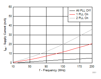
| IDD | Supply current (see Figure 1) | All outputs off, fCLK = 27 MHz, fVCO = 135 MHz; fOUT = 27 MHz |
All PLLS on | 20 | mA | ||
| Per PLL | 9 | ||||||
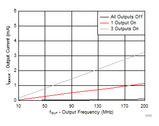
| IDDOUT | Supply current (see Figure 2) | No load, all outputs on, fOUT = 27 MHz |
VDDOUT = 1.8 V | 1 | mA | ||
| IDDPD | Power-down current. Every circuit powered down except SDA/SCL | fIN = 0 MHz, | VDD = 1.9 V | 30 | μA | ||
| VPUC | Supply voltage VDD threshold for power-up control circuit | 0.85 | 1.45 | V | |||
| fVCO | VCO frequency range of PLL | 80 | 201 | MHz | |||
| fOUT | LVCMOS output frequency | VDDOUT = 1.8 V | 201 | MHz | |||
| LVCMOS PARAMETER | |||||||
| VIK | LVCMOS input voltage | VDD = 1.7 V; IS = –18 mA | –1.2 | V | |||
| II | LVCMOS input current | VI = 0 V or VDD; VDD = 1.9 V | ±5 | μA | |||
| IIH | LVCMOS input current for S0/S1/S2 | VI = VDD; VDD = 1.9 V | 5 | μA | |||
| IIL | LVCMOS Input current for S0/S1/S2 | VI = 0 V; VDD = 1.9 V | –4 | μA | |||
| CI | Input capacitance at Xin/Clk | VIClk = 0 V or VDD | 6 | pF | |||
| Input capacitance at Xout | VIXout = 0 V or VDD | 2 | |||||
| Input capacitance at S0/S1/S2 | VIS = 0 V or VDD | 3 | |||||
| LVCMOS PARAMETER for VDDOUT = 1.8 V – MODE | |||||||
| VOH | LVCMOS high-level output voltage | VDDOUT = 1.7 V, IOH = –0.1 mA | 1.6 | V | |||
| VDDOUT = 1.7 V, IOH = –4 mA | 1.4 | ||||||
| VDDOUT = 1.7 V, IOH = –8 mA | 1.1 | ||||||
| VOL | LVCMOS low-level output voltage | VDDOUT = 1.7 V, IOL = 0.1 mA | 0.1 | V | |||
| VDDOUT = 1.7 V, IOL = 4 mA | 0.3 | ||||||
| VDDOUT = 1.7 V, IOL = 8 mA | 0.6 | ||||||
| tPLH, tPHL | Propagation delay | All PLL bypass | 2.6 | ns | |||
| tr/tf | Rise and fall time | VDDOUT = 1.8 V (20%–80%) | 0.7 | ns | |||
| tjit(cc) | Cycle-to-cycle jitter (2) (3) | 1 PLL switching, Y1-to-Y2 | 80 | 110 | ps | ||
| 2 PLL switching, Y1-to-Y4 | 130 | 200 | |||||
| tjit(per) | Peak-to-peak period jitter (3) | 1 PLL switching, Y1-to-Y2 | 100 | 130 | ps | ||
| 2 PLL switching, Y1-to-Y4 | 150 | 220 | |||||
| tsk(o) | Output skew(4) | fOUT = 50 MHz; Y1-to-Y2 | 50 | ps | |||
| fOUT = 50 MHz; Y1-to-Y4 | 110 | ||||||
| odc | Output duty cycle(5) | fVCO = 100 MHz; Pdiv = 1 | 45% | 55% | |||
| SDA/SCL PARAMETER | |||||||
| VIK | SCL and SDA input clamp voltage | VDD = 1.7 V; II = –18 mA | –1.2 | V | |||
| IIH | SCL and SDA input current | VI = VDD; VDD = 1.9 V | ±10 | μA | |||
| VIH | SDA/SCL input high voltage(6) | 0.7 VDD | V | ||||
| VIL | SDA/SCL input low voltage(6) | 0.3 VDD | V | ||||
| VOL | SDA low-level output voltage | IOL = 3 mA VDD = 1.7 V | 0.2 VDD | V | |||
| CI | SCL/SDA Input capacitance | VI = 0 V or VDD | 3 | 10 | pF | ||
(1) All typical values are at respective nominal VDD.
(2) 10,000 cycles
(3) Jitter depends on configuration. Jitter data is for input frequency = 27 MHz, fVCO = 135 MHz, fOUT = 27 MHz. fOUT = 3.072 MHz or input frequency = 27 MHz, fVCO = 108 MHz, fOUT = 27 MHz. fOUT = 16.384 MHz, fOUT = 25 MHz, fOUT = 74.25 MHz, fOUT = 48 MHz
(4) The tsk(o) specification is only valid for equal loading of each bank of outputs, and the outputs are generated from the same divider, data sampled on rising edge (tr).
(5) odc depends on output rise- and fall time (tr/tf).
(6) SDA and SCL pins are 3.3-V tolerant.
7.6 CLK_IN Timing Requirements
over recommended ranges of supply voltage, load, and operating free-air temperature| MIN | NOM | MAX | UNIT | |||
|---|---|---|---|---|---|---|
| fCLK | LVCMOS clock input frequency | PLL bypass mode | 0 | 130 | MHz | |
| PLL mode | 8 | 130 | ||||
| tr / tf | Rise and fall time CLK signal (20% to 80%) | 3 | ns | |||
| dutyCLK | Duty cycle CLK at VDD / 2 | 40% | 60% | |||
7.7 SDA/SCL Timing Requirements
| (SeeFigure 5) | STANDARD MODE | FAST MODE | UNIT | |||
|---|---|---|---|---|---|---|
| MIN | MAX | MIN | MAX | |||
| fSCL | SCL clock frequency | 0 | 100 | 0 | 400 | kHz |
| tsu(START) | START setup time (SCL high before SDA low) | 4.7 | 0.6 | μs | ||
| th(START) | START hold time (SCL low after SDA low) | 4 | 0.6 | μs | ||
| tw(SCLL) | SCL low-pulse duration | 4.7 | 1.3 | μs | ||
| tw(SCLH) | SCL high-pulse duration | 4 | 0.6 | μs | ||
| th(SDA) | SDA hold time (SDA valid after SCL low) | 0 | 3.45 | 0 | 0.9 | μs |
| tsu(SDA) | SDA setup time | 250 | 100 | ns | ||
| tr | SCL/SDA input rise time | 1000 | 300 | ns | ||
| tf | SCL/SDA input fall time | 300 | 300 | ns | ||
| tsu(STOP) | STOP setup time | 4 | 0.6 | μs | ||
| tBUS | Bus free time between a STOP and START condition | 4.7 | 1.3 | μs | ||
7.8 EEPROM Specification
| MIN | TYP | MAX | UNIT | ||
|---|---|---|---|---|---|
| EEcyc | Programming cycles of EEPROM | 100 | 1000 | cycles | |
| EEret | Data retention | 10 | years | ||
7.9 Typical Characteristics

