ZHCSTF3I June 2007 – August 2024 CDCE913 , CDCEL913
PRODUCTION DATA
- 1
- 1 特性
- 2 应用
- 3 说明
- 4 Pin Configuration and Functions
-
5 Specifications
- 5.1 Absolute Maximum Ratings
- 5.2 ESD Ratings
- 5.3 Recommended Operating Conditions
- 5.4 Thermal Information
- 5.5 Electrical Characteristics
- 5.6 EEPROM Specification
- 5.7 Timing Requirements: CLK_IN
- 5.8 Timing Requirements: SDA/SCL #GUID-DE171716-D3A0-4375-A25C-58C636304087/SCAS849414
- 5.9 Typical Characteristics
- 6 Parameter Measurement Information
- 7 Detailed Description
- 8 Application and Implementation
- 9 Register Maps
- 10Device and Documentation Support
- 11Revision History
- 12Mechanical, Packaging, and Orderable Information
8.2.2.3 Crystal Oscillator Start-up
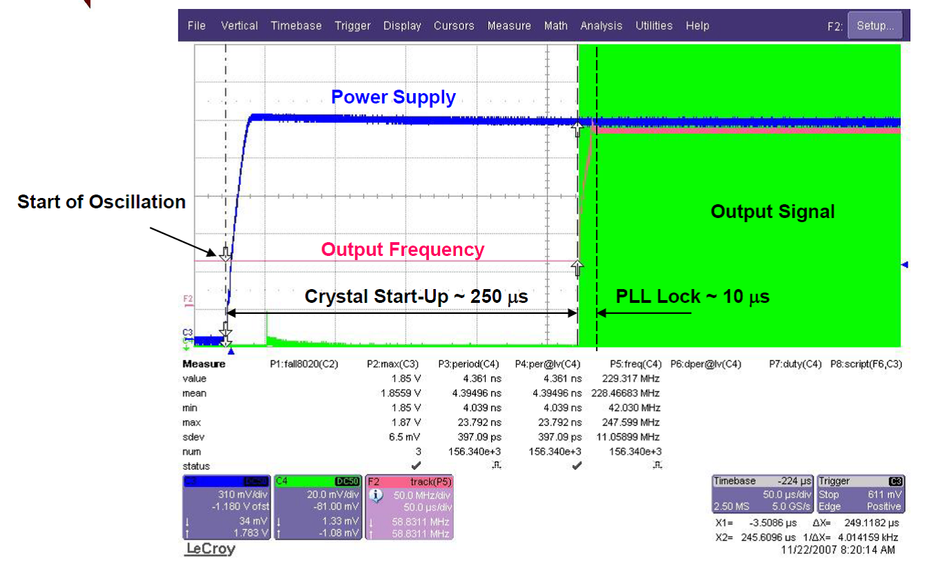
When the CDCE913 or CDCEL913 is used as a crystal buffer, crystal oscillator start-up dominates the start-up time compared to the internal PLL lock time. The following diagram shows the oscillator start-up sequence for a 27-MHz crystal input with an 8-pF load. The start-up time for the crystal is in the order of approximately 250 µs compared to approximately 10 µs of lock time. In general, lock time is an order of magnitude less compared to the crystal start-up time.
 Figure 8-5 Crystal Oscillator Start-Up vs PLL Lock Time