SCAS892C February 2010 – December 2016 CDCE937-Q1 , CDCEL937-Q1
PRODUCTION DATA.
- 1 Features
- 2 Applications
- 3 Description
- 4 Revision History
- 5 Description (continued)
- 6 Device Comparison Table
- 7 Pin Configuration and Functions
- 8 Specifications
- 9 Parameter Measurement Information
-
10Detailed Description
- 10.1 Overview
- 10.2 Functional Block Diagram
- 10.3 Feature Description
- 10.4 Device Functional Modes
- 10.5
Programming
- 10.5.1 Data Protocol
- 10.5.2 Command Code Definition
- 10.5.3 Generic Programming Sequence
- 10.5.4 Byte Write Programming Sequence
- 10.5.5 Byte Read Programming Sequence
- 10.5.6 Block Write Programming Sequence
- 10.5.7 Block Read Programming Sequence
- 10.5.8 Timing Diagram for the SDA and SCL Serial Control Interface
- 10.5.9 SDA and SCL Hardware Interface
- 10.6 Register Maps
- 11Application and Implementation
- 12Power Supply Recommendations
- 13Layout
- 14Device and Documentation Support
- 15Mechanical, Packaging, and Orderable Information
11 Application and Implementation
NOTE
Information in the following applications sections is not part of the TI component specification, and TI does not warrant its accuracy or completeness. TI’s customers are responsible for determining suitability of components for their purposes. Customers should validate and test their design implementation to confirm system functionality.
11.1 Application Information
The CDCE937-Q1 device is an easy-to-use, high-performance, programmable CMOS clock synthesizer which can be used as a crystal buffer, clock synthesizer with separate output supply pin. The CDCE937-Q1 device features an on-chip loop filter and spread-spectrum modulation. Programming can be done through the I2C interface, or previously saved settings can be loaded from on-chip EEPROM. The pins S0, S1, and S2 can be programmed as control pins to select various output settings. This section shows some examples of using the CDCE937-Q1 device in various applications.
11.2 Typical Application
Figure 14 shows the use of the CDCE937-Q1 device in an infotainment system, such as in head unit or telematics applications, using a 1.8-V single supply. Note that bypass capacitors are not shown in this schematic.
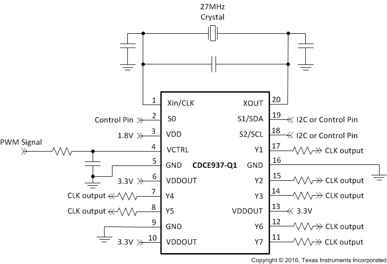 Figure 14. Single-Chip Solution Using a CDCE937-Q1 Device for Generating Clocking Frequencies
11.2.1 Design Requirements
The CDCE937-Q1 device supports spread-spectrum clocking (SSC) with multiple control parameters:
- Modulation amount (%)
- Modulation frequency (>20 kHz)
- Modulation shape (triangular, hershey, and others)
- Center spread or down spread (± or –)
For sample calculations of PLL constants, see PLL Multiplier or Divider Definition.
 Figure 15. Modulation Frequency (fm) and Modulation Amount
11.2.2 Detailed Design Procedure
11.2.2.1 Spread-Spectrum Clock (SSC)
Spread-spectrum modulation is a method to spread emitted energy over a larger bandwidth. In clocking, spread spectrum can reduce electromagnetic interference (EMI) by reducing the level of emission from clock distribution network.
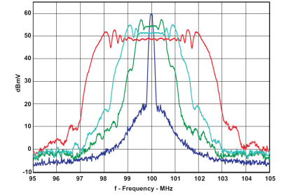
Spread spectrum clocking can be used to help reduce EMI to meet design specifications. For example, a specified EMI threshold of 55 dB/mV would require ±1% spread spectrum clocking to meet this requirement.
11.2.2.2 PLL Multiplier or Divider Definition
At a given input frequency (ƒIN), the output frequency (ƒOUT) of the CDCEx937-Q1 can be calculated with Equation 1.

where
- M (1 to 511) and N (1 to 4095) are the multiplier/divide values of the PLL
- Pdiv (1 to 127) is the output divider
The target VCO frequency (ƒVCO) of each PLL can be calculated with Equation 2.

The PLL internally operates as fractional divider and requires the following multiplier and divider settings:
N
P = 4 – int 
Q = int 
R = N′ – M × Q
where
N′ = N × 2P
N ≥ M
100 MHz < ƒVCO > 200 MHz
| Example: | |||
| for ƒIN = 27 MHz; M = 1; N = 4; Pdiv = 2; | for ƒIN = 27 MHz; M = 2; N = 11; Pdiv = 2; | ||
| → | fOUT = 54 MHz | → | fOUT = 74.25 MHz |
| → | fVCO = 108 MHz | → | fVCO = 148.50 MHz |
| → | P = 4 – int(log24) = 4 – 2 = 2 | → | P = 4 – int(log25.5) = 4 – 2 = 2 |
| → | N′ = 4 × 22 = 16 | → | N′ = 11 × 22 = 44 |
| → | Q = int(16) = 16 | → | Q = int(22) = 22 |
| → | R = 16 – 16 = 0 | → | R = 44 – 44 = 0 |
The values for P, Q, R, and N’ is automatically calculated when using TI Pro-Clock™ software.
11.2.2.3 Crystal Oscillator Start-Up
When the CDCE937-Q1 or CDCEL937-Q1 device is used as a crystal buffer, crystal oscillator start-up dominates the start-up time compared to the internal PLL lock time. The following diagram shows the oscillator start-up sequence for a 27-MHz crystal input with an 8-pF load. The start-up time for the crystal is on the order of approximately 250 µs compared to approximately 10 µs of lock time. In general, lock time is an order of magnitude less compared to the crystal start-up time.
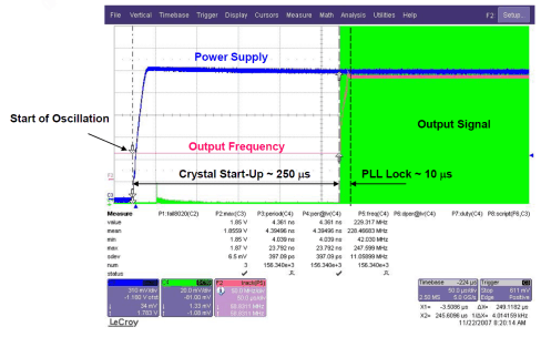 Figure 17. Crystal Oscillator Start-Up vs PLL Lock Time
11.2.2.4 Frequency Adjustment With Crystal Oscillator Pulling
The frequency for the CDCE937-Q1 or CDCEL937-Q1 device is adjusted for media and other applications with the VCXO control input Vctr. If a PWM-modulated signal is used as a control signal for the VCXO, an external filter is required.
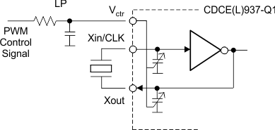 Figure 18. Frequency Adjustment Using PWM Input to the VCXO Control
11.2.2.5 Unused Inputs and Outputs
If VCXO-pulling functionality is not required, Vctr must be left floating. All other unused inputs must be set to GND. Unused outputs must be left floating.
If one output block is not used, TI recommends disabling it. However, TI recommends providing a supply for all output blocks, even if they are disabled.
11.2.2.6 Switching Between XO and VCXO Mode
When the CDCEx937-Q1 device is in the crystal-oscillator or VCXO configuration, the internal capacitors require different internal capacitance. The following steps are recommended to switch to VCXO mode when the configuration for the on-chip capacitor is still set for XO mode. To center the output frequency to 0 ppm:
- While in XO mode, put Vctr = VDD / 2
- Switch from XO mode to VCXO mode
- Program the internal capacitors to obtain 0 ppm at the output.
11.2.3 Application Curves
Figure 19, Figure 20, Figure 21, and Figure 22 show CDCE937-Q1 measurements with the SSC feature enabled. Device configuration: 27-MHz input, 27-MHz output.
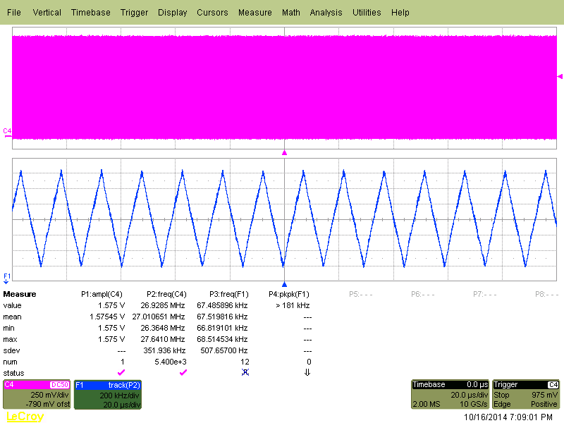 Figure 19. fOUT = 27 MHz,
VCO frequency < 125 MHz, SSC (2% Center)
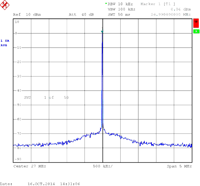 Figure 21. Output Spectrum With SSC Off
 Figure 20. fOUT = 27 MHz,
VCO frequency > 175 MHz, SSC (1%, Center)
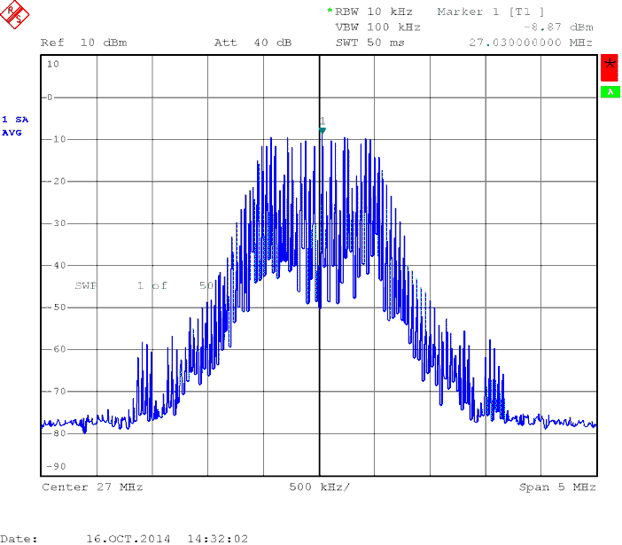 Figure 22. Output Spectrum With SSC On,
2% Center