SCAS892C February 2010 – December 2016 CDCE937-Q1 , CDCEL937-Q1
PRODUCTION DATA.
- 1 Features
- 2 Applications
- 3 Description
- 4 Revision History
- 5 Description (continued)
- 6 Device Comparison Table
- 7 Pin Configuration and Functions
- 8 Specifications
- 9 Parameter Measurement Information
-
10Detailed Description
- 10.1 Overview
- 10.2 Functional Block Diagram
- 10.3 Feature Description
- 10.4 Device Functional Modes
- 10.5
Programming
- 10.5.1 Data Protocol
- 10.5.2 Command Code Definition
- 10.5.3 Generic Programming Sequence
- 10.5.4 Byte Write Programming Sequence
- 10.5.5 Byte Read Programming Sequence
- 10.5.6 Block Write Programming Sequence
- 10.5.7 Block Read Programming Sequence
- 10.5.8 Timing Diagram for the SDA and SCL Serial Control Interface
- 10.5.9 SDA and SCL Hardware Interface
- 10.6 Register Maps
- 11Application and Implementation
- 12Power Supply Recommendations
- 13Layout
- 14Device and Documentation Support
- 15Mechanical, Packaging, and Orderable Information
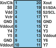
7 Pin Configuration and Functions
PW Package
20-Pin TSSOP
Top View

Pin Functions
| PIN | TYPE(1) | DESCRIPTION | |
|---|---|---|---|
| NO. | NAME | ||
| 1 | Xin/CLK | I | Crystal oscillator input or LVCMOS clock input (selectable through SDA and SCL bus) |
| 2 | S0 | I | User-programmable control input S0; LVCMOS inputs; Internal pullup 500 k |
| 3 | VDD | P | 1.8-V power supply for the device |
| 4 | VCtrl | I | VCXO control voltage (leave open or pull up to approximately 500 k when not used) |
| 5 | GND | G | Ground |
| 6 | Vddout | P | CDCE937-Q1: 3.3-V or 2.5-V supply for all outputs CDCEL937-Q1: 1.8-V supply for all outputs |
| 7 | Y4 | O | LVCMOS outputs |
| 8 | Y5 | O | LVCMOS outputs |
| 9 | GND | G | Ground |
| 10 | Vddout | P | CDCE937-Q1: 3.3-V or 2.5-V supply for all outputs CDCEL937-Q1: 1.8-V supply for all outputs |
| 11 | Y7 | O | LVCMOS outputs |
| 12 | Y6 | O | LVCMOS outputs |
| 13 | Vddout | P | CDCE937-Q1: 3.3-V or 2.5-V supply for all outputs CDCEL937-Q1: 1.8-V supply for all outputs |
| 14 | Y3 | O | LVCMOS outputs |
| 15 | Y2 | O | LVCMOS outputs |
| 16 | GND | G | Ground |
| 17 | Y1 | O | LVCMOS outputs |
| 18 | SCL/S2 | I | SCL: serial clock input(default configuration), LVCMOS internal pullup 500 k; or S2: user-programmable control input, LVCMOS inputs, and internal pullup 500 k |
| 19 | SDA/S1 | I/O or I | SDA: bidirectional serial data input/output (default configuration). LVCMOS internal pullup 500 k; or S1: user-programmable control input, LVCMOS inputs, and internal pullup 500 k |
| 20 | Xout | O | Crystal oscillator output (leave open or pull up to approximately 500 k when not used) |
(1) G = Ground, I = Input, O = Output, P = Power