ZHCSGV7F July 2017 – January 2024 CDCI6214
PRODUCTION DATA
- 1
- 1 特性
- 2 应用
- 3 说明
- 4 Device Comparison
- 5 Pin Configuration and Functions
-
6 Specifications
- 6.1 Absolute Maximum Ratings
- 6.2 ESD Ratings
- 6.3 Recommended Operating Conditions
- 6.4 Thermal Information
- 6.5 EEPROM Characteristics
- 6.6 Reference Input, Single-Ended and Differential Mode Characteristics (REFP, REFN, FB_P, FB_N)
- 6.7 Reference Input, Crystal Mode Characteristics (XIN, XOUT)
- 6.8 General-Purpose Input and Output Characteristics (GPIO[4:1], SYNC/RESETN)
- 6.9 Triple Level Input Characteristics (EEPROMSEL, REFSEL)
- 6.10 Reference Mux Characteristics
- 6.11 Phase-Locked Loop Characteristics
- 6.12 Closed-Loop Output Jitter Characteristics
- 6.13 Output Mux Characteristics
- 6.14 LVCMOS Output Characteristics
- 6.15 HCSL Output Characteristics
- 6.16 LVDS DC-Coupled Output Characteristics
- 6.17 Programmable Differential AC-Coupled Output Characteristics
- 6.18 Output Skew and Delay Characteristics
- 6.19 Output Synchronization Characteristics
- 6.20 Timing Characteristics
- 6.21 I2C-Compatible Serial Interface Characteristics (SDA/GPIO2, SCL/GPIO3)
- 6.22 Timing Requirements, I2C-Compatible Serial Interface (SDA/GPIO2, SCL/GPIO3)
- 6.23 Power Supply Characteristics
- 6.24 Typical Characteristics
- 7 Parameter Measurement Information
-
8 Detailed Description
- 8.1 Overview
- 8.2 Functional Block Diagram
- 8.3 Feature Description
- 8.4 Device Functional Modes
- 8.5 Programming
- 9 Application and Implementation
- 10Register Maps
- 11Device and Documentation Support
- 12Revision History
- 13Mechanical, Packaging, and Orderable Information
9.4 Initialization Setup
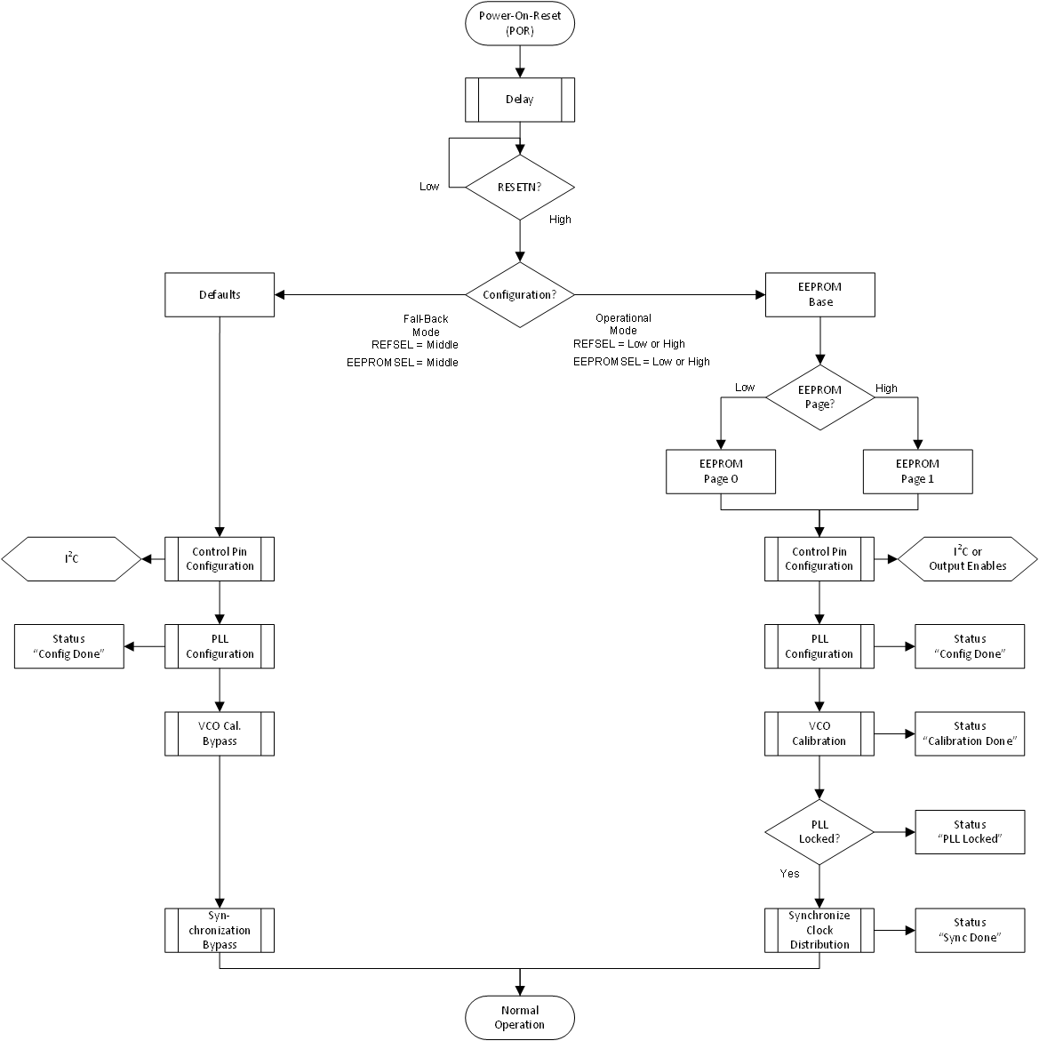
The device digital logic starts after the internal power-on-release circuit triggered (POR). The digital core is connected to the VDDREF domain. The EEPROM settings are loaded into the device registers and the new settings applied to the device. The EEPROM page is selected according to the EEPROMSEL pin logic level. A low level loads page 0, and a logic high level loads page 1. By default, the differential outputs are muted for the initial VCO calibration and PLL lock process. After the PLL circuit achieved a phase lock to the input reference, the output dividers are synchronized and then released to operation. By default, pin 8 is configured as RESETN pin (see gpio0_dir_sel and gpio0_input_sel). The start of the initialization sequence, as well the as serial interface, can be kept in reset using RESETN= LOW. When pin 8 is not configured as RESETN, the device initialization relies on the POR triggered by application of VDDREF.
 Figure 9-5 Initialization Flow Chart
The pins 8, 11, 12, 19, and 20 are general-purpose inputs and outputs (GPIO). The functions are determined through the register settings saved in the selected EEPROM page. See Generic0, Generic1, and Ceneric2for the relevant bit-fields.
The EEPROM allows to choose between two modes of operation: pin Mode and serial interface mode. This is done using mode.