SCAS895B May 2010 – February 2017 CDCLVC1102 , CDCLVC1103 , CDCLVC1104 , CDCLVC1106 , CDCLVC1108 , CDCLVC1110 , CDCLVC1112
PRODUCTION DATA.
- 1 Features
- 2 Applications
- 3 Description
- 4 Revision History
- 5 Pin Configuration and Functions
- 6 Specifications
- 7 Parameter Measurement Information
- 8 Detailed Description
- 9 Application and Implementation
- 10Power Supply Recommendations
- 11Layout
- 12Device and Documentation Support
- 13Mechanical, Packaging, and Orderable Information
9 Application and Implementation
NOTE
Information in the following applications sections is not part of the TI component specification, and TI does not warrant its accuracy or completeness. TI’s customers are responsible for determining suitability of components for their purposes. Customers should validate and test their design implementation to confirm system functionality.
9.1 Application Information
The CDCLVC11xx family is a low additive jitter LVCMOS buffer solution that can operate up to 250 MHz at and 180 MHz at VDD = 2.5 V. Low output skew as well as the ability for asynchronous output enable is featured to simultaneously enable or disable buffered clock outputs as necessary in the application.
9.2 Typical Application
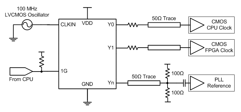
 Figure 10. Example System Configuration
9.2.1 Design Requirements
The CDCLVC11xx shown in Figure 10 is configured to fan out a 100-MHz signal from a local LVCMOS oscillator. The CPU is configured to control the output state through 1G.
The configuration example is driving three LVCMOS receivers in a backplane application with the following properties:
- The CPU clock can accept a full swing DC-coupled LVCMOS signal. A series resistor is placed near the CDCLVC11xx to closely match the characteristic impedance of the trace to minimize reflections.
- The FPGA clock is similarly DC-coupled with an appropriate series resistor placed near the CDCLVC11xx.
- The PLL in this example can accept a lower amplitude signal, so a Thevenin's equivalent termination is used. The PLL receiver features internal biasing, so AC coupling can be used when common-mode voltage is mismatched.
9.2.2 Detailed Design Procedure
Refer to Figure 5 and the Electrical Characteristics table to determine the appropriate series resistance needed for matching the output impedance of the CDCLVC11xx to that of the characteristic impedance of the transmission line.
Unused outputs can be left floating. See the Power Supply Recommendations section for recommended filtering techniques.
9.2.3 Application Curves
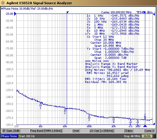
 Figure 11. CDCLVC11xx Reference Phase Noise 26 fs
 (12 kHz to 20 MHz)
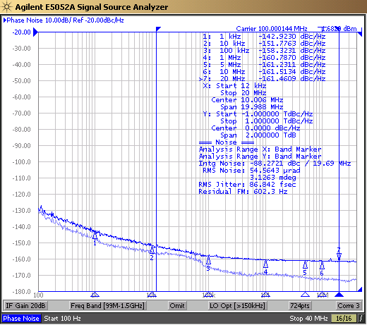
 Figure 12. CDCLVC11xx Output Phase Noise 86 fs
 (12 kHz to 20 MHz)
The low additive jitter of the CDCLVC11xx can be shown in the previous application example. The low-noise 100-MHz XO with 26-fs RMS jitter drives the CDCLVC11xx, resulting in 86-fs RMS jitter when integrated from 12 kHz to 20 MHz. The resultant additive jitter is a low 82-fs RMS for this configuration.