SCAS895B May 2010 – February 2017 CDCLVC1102 , CDCLVC1103 , CDCLVC1104 , CDCLVC1106 , CDCLVC1108 , CDCLVC1110 , CDCLVC1112
PRODUCTION DATA.
- 1 Features
- 2 Applications
- 3 Description
- 4 Revision History
- 5 Pin Configuration and Functions
- 6 Specifications
- 7 Parameter Measurement Information
- 8 Detailed Description
- 9 Application and Implementation
- 10Power Supply Recommendations
- 11Layout
- 12Device and Documentation Support
- 13Mechanical, Packaging, and Orderable Information
11 Layout
11.1 Layout Guidelines
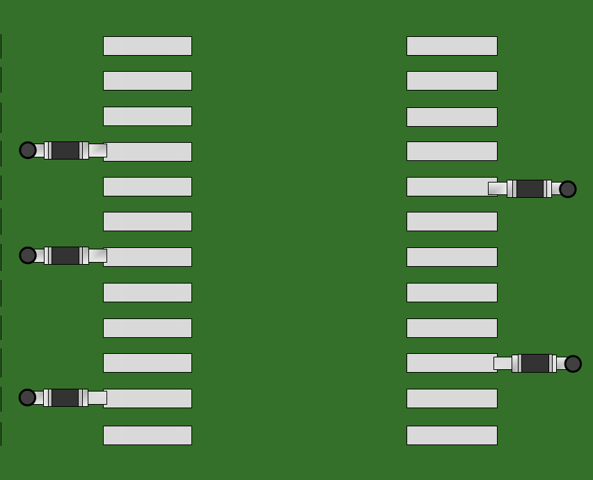
Figure 14 shows a conceptual layout detailing recommended placement of power supply bypass capacitors. For component side mounting, use 0402 body size capacitors to facilitate signal routing. Keep the connections between the bypass capacitors and the power supply on the device as short as possible. Ground the other side of the capacitor using a low-impedance connection to the ground plane.
11.2 Layout Example
 Figure 14. PCB Conceptual Layout