SCAS899A August 2010 – October 2016 CDCLVD1208
PRODUCTION DATA.
- 1 Features
- 2 Applications
- 3 Description
- 4 Revision History
- 5 Pin Configuration and Functions
- 6 Specifications
- 7 Parameter Measurement Information
- 8 Detailed Description
- 9 Application and Implementation
- 10Power Supply Recommendations
- 11Layout
- 12Device and Documentation Support
- 13Mechanical, Packaging, and Orderable Information
7 Parameter Measurement Information
 Figure 3. LVDS Output DC Configuration During Device Test
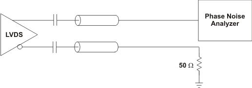
 Figure 4. LVDS Output AC Configuration During Device Test
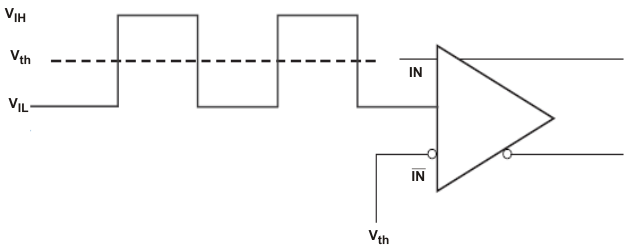
 Figure 5. DC-Coupled LVCMOS Input During Device Test
 Figure 6. Output Voltage and Rise/Fall Time

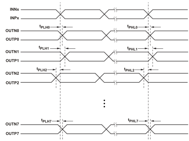
A. Output skew is calculated as the greater of the following: the difference between the fastest and the slowest tPLHn or the difference between the fastest and the slowest tPHLn (n = 0, 1, 2, ..7)
B. Part to part skew is calculated as the greater of the following: the difference between the fastest and the slowest tPLHn or the difference between the fastest and the slowest tPHLn across multiple devices (n = 0, 1, 2, ..7)
Figure 7. Output Skew and Part-to-Part Skew
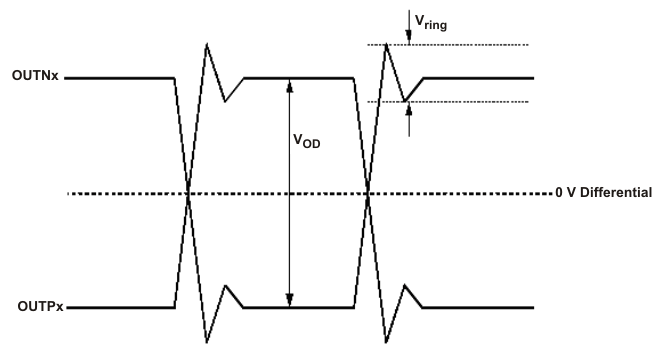
 Figure 8. Output Overshoot and Undershoot
 Figure 9. Output AC Common Mode