SCAS901D September 2010 – November 2017 CDCLVD1212
PRODUCTION DATA.
- 1 Features
- 2 Applications
- 3 Description
- 4 Revision History
- 5 Pin Configuration and Functions
- 6 Specifications
- 7 Parameter Measurement Information
- 8 Detailed Description
- 9 Application and Implementation
- 10Power Supply Recommendations
- 11Layout
- 12Device and Documentation Support
- 13Mechanical, Packaging, and Orderable Information
8 Detailed Description
8.1 Overview
The CDCLVD1212 LVDS drivers use CMOS transistors to control the output current. Therefore, proper biasing and termination are required to ensure correct operation of the device and to maximize signal integrity.
The proper LVDS termination for signal integrity over two 50-Ω lines is 100 Ω between the outputs on the receiver end. Either DC-coupled termination or AC-coupled termination can be used for LVDS outputs. TI recommends placing a termination resistor close to the receiver. If the receiver is internally biased to a voltage different than the output common-mode voltage of the CDCLVD1212, AC-coupling must be used. If the LVDS receiver has internal 100-Ω termination, external termination must be omitted.
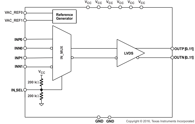
8.2 Functional Block Diagram

8.3 Feature Description
The CDCLVD1212 is a low additive jitter LVDS fan-out buffer that can generate twelve copies of two selectable LVPECL, LVDS, or LVCMOS inputs. The CDCLVD1212 can accept reference clock frequencies up to 800 MHz while providing low output skew.
8.4 Device Functional Modes
The two inputs of the CDCLVD1212 are internally muxed together and can be selected through the control pin (see Table 1). Unused inputs and outputs can be left floating to reduce overall component cost. Both AC- and DC-coupling schemes can be used with the CDCLVD1212 to provide greater system flexibility.
Table 1. Input Selection Table
| IN_SEL | ACTIVE CLOCK INPUT |
|---|---|
| 0 | INP0, INN0 |
| 1 | INP1, INN1 |
| Open | None(1) |
8.4.1 LVDS Output Termination
Unused outputs can be left open without connecting any trace to the output pins.
The CDCLVD1212 can be connected to LVDS receiver inputs with DC- and AC-coupling as shown in Figure 10 and Figure 11 (respectively).
 Figure 10. Output DC Termination
 Figure 11. Output AC Termination (With the Receiver Internally Biased)
8.4.2 Input Termination
The CDCLVD1212 inputs can be interfaced with LVDS, LVPECL, or LVCMOS drivers.
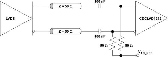
LVDS drivers can be connected to CDCLVD1212 inputs with DC- or AC-coupling as shown in Figure 12 and Figure 13 (respectively).
 Figure 12. LVDS Clock Driver Connected to CDCLVD1212 Input (DC-Coupled)
 Figure 13. LVDS Clock Driver Connected to CDCLVD1212 Input (AC-Coupled)
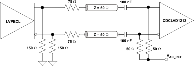
Figure 14 shows how to connect LVPECL inputs to the CDCLVD1212. The series resistors are required to reduce the LVPECL signal swing if the signal swing is >1.6 VPP.
 Figure 14. LVPECL Clock Driver Connected to CDCLVD1212 Input
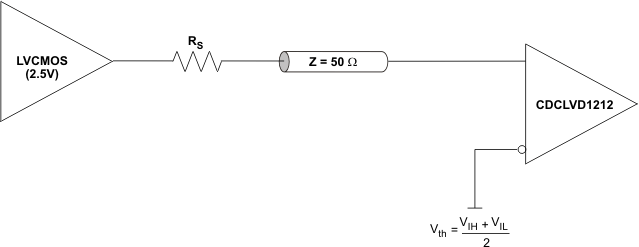
Figure 15 illustrates how to couple a 2.5-V LVCMOS clock input to the CDCLVD1212 directly. The series resistance, RS, must be placed close to the LVCMOS driver if required. 3.3-V LVCMOS clock input swing must be limited to VIH ≤ VCC.
 Figure 15. 2.5-V LVCMOS Clock Driver Connected to CDCLVD1212 Input
For unused input, TI recommends grounding both input pins (INP, INN) using 1-kΩ resistors.