SCAS884D August 2009 – December 2015 CDCLVP1102
PRODUCTION DATA.
- 1 Features
- 2 Applications
- 3 Description
- 4 Revision History
- 5 Pin Configuration and Functions
-
6 Specifications
- 6.1 Absolute Maximum Ratings
- 6.2 ESD Ratings
- 6.3 Recommended Operating Conditions
- 6.4 Thermal Information
- 6.5 Electrical Characteristics: LVCMOS Input
- 6.6 Electrical Characteristics: Differential Input
- 6.7 Electrical Characteristics: LVPECL Output
- 6.8 Electrical Characteristics: LVPECL Output
- 6.9 Typical Characteristics
- 7 Parameter Measurement Information
- 8 Detailed Description
- 9 Application and Implementation
- 10Power Supply Recommendations
- 11Layout
- 12Device and Documentation Support
- 13Mechanical, Packaging, and Orderable Information
8 Detailed Description
8.1 Overview
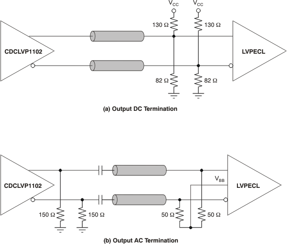
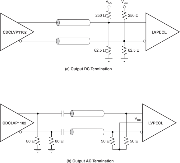
The CDCLVP1102 is an open emitter for LVPECL outputs. Therefore, proper biasing and termination are required to ensure correct operation of the device and to minimize signal integrity. The proper termination for LVPECL outputs is 50 Ω to (VCC –2) V, but this DC voltage is not readily available on PCB. Therefore, a Thevenin equivalent circuit is worked out for the LVPECL termination in both direct-coupled (DC) and AC coupled configurations. These configurations are shown in Figure 12 for VCC = 2.5 V and Figure 13 for VCC = 3.3 V, respectively. It is recommended to place all resistive components close to either the driver end or the receiver end. If the supply voltage for the driver and receiver is different, AC coupling is required.
8.2 Functional Block Diagram

8.3 Feature Description
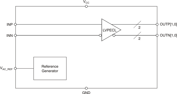
The CDCLVP1102 is a low additive jitter universal to LVPECL fan out buffer with 2 outputs and 1 input. The small package, low output skew, and low additive jitter make for a flexible device in demanding applications.
8.4 Device Functional Modes
The CDCLVP1102 is an open emitter for LVPECL outputs. Therefore, proper biasing and termination are required to ensure correct operation of the device and to minimize signal integrity. The proper termination for LVPECL outputs is 50 Ω to (VCC –2) V, but this dc voltage is not readily available on PCB. Therefore, a Thevenin equivalent circuit is worked out for the LVPECL termination in both direct-coupled (DC) and AC-coupled configurations. These configurations are shown in Figure 12a and b for VCC = 2.5 V and Figure 13a and b for VCC = 3.3 V, respectively. It is recommended to place all resistive components close to either the driver end or the receiver end. If the supply voltage for the driver and receiver is different, ac coupling is required.
8.4.1 LVPECL Output Termination
 Figure 13. LVPECL Output DC and AC Termination for VCC = 3.3 V
8.4.2 Input Termination
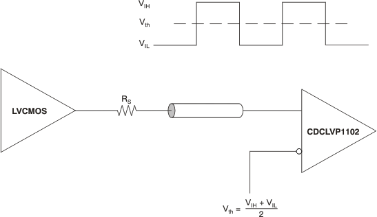
The CDCLVP1102 inputs can be interfaced with LVPECL, LVDS, or LVCMOS drivers. Figure 14 illustrates how to dc couple an LVCMOS input to the CDCLVP1102. The series resistance (RS) should be placed close to the LVCMOS driver; its value is calculated as the difference between the transmission line impedance and the driver output impedance.
 Figure 14. DC-Coupled LVCMOS Input to CDCLVP1102
Figure 15 shows how to dc couple LVDS inputs to the CDCLVP1102. Figure 16 and Figure 17 describe the method of dc coupling LVPECL inputs to the CDCLVP1102 for VCC = 2.5 V and VCC = 3.3 V, respectively.
 Figure 15. DC-Coupled LVDS Inputs to CDCLVP1102
Figure 18 and Figure 19 show the technique of AC coupling differential inputs to the CDCLVP1102 for VCC = 2.5 V and VCC = 3.3 V, respectively. It is recommended to place all resistive components close to either the driver end or the receiver end. If the supply voltages of the driver and receiver are different, ac coupling is required.
 Figure 18. AC-Coupled Differential Inputs to CDCLVP1102 (VCC = 2.5 V)
 Figure 19. AC-Coupled Differential Inputs to CDCLVP1102 (VCC = 3.3 V)


