SCAS884D August   2009  – December 2015 CDCLVP1102

PRODUCTION DATA.  

  1. Features
  2. Applications
  3. Description
  4. Revision History
  5. Pin Configuration and Functions
  6. Specifications
    1. 6.1 Absolute Maximum Ratings
    2. 6.2 ESD Ratings
    3. 6.3 Recommended Operating Conditions
    4. 6.4 Thermal Information
    5. 6.5 Electrical Characteristics: LVCMOS Input
    6. 6.6 Electrical Characteristics: Differential Input
    7. 6.7 Electrical Characteristics: LVPECL Output
    8. 6.8 Electrical Characteristics: LVPECL Output
    9. 6.9 Typical Characteristics
  7. Parameter Measurement Information
    1. 7.1 Test Configurations
  8. Detailed Description
    1. 8.1 Overview
    2. 8.2 Functional Block Diagram
    3. 8.3 Feature Description
    4. 8.4 Device Functional Modes
      1. 8.4.1 LVPECL Output Termination
      2. 8.4.2 Input Termination
  9. Application and Implementation
    1. 9.1 Application Information
    2. 9.2 Typical Application
      1. 9.2.1 Fanout Buffer for Line Card Application
        1. 9.2.1.1 Design Requirements
        2. 9.2.1.2 Detailed Design Procedure
        3. 9.2.1.3 Application Curves
  10. 10Power Supply Recommendations
  11. 11Layout
    1. 11.1 Layout Guidelines
    2. 11.2 Layout Example
    3. 11.3 Thermal Considerations
  12. 12Device and Documentation Support
    1. 12.1 Documentation Support
      1. 12.1.1 Related Documentation
    2. 12.2 Community Resources
    3. 12.3 Trademarks
    4. 12.4 Electrostatic Discharge Caution
    5. 12.5 Glossary
  13. 13Mechanical, Packaging, and Orderable Information

封装选项

机械数据 (封装 | 引脚)
散热焊盘机械数据 (封装 | 引脚)
订购信息

5 Pin Configuration and Functions

RGT Package
16-Pin VQFN
Top View
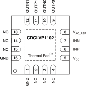
CDCLVP1102 po_cas884.gif
1. Thermal pad must be soldered to ground.

Pin Functions

PIN TYPE DESCRIPTION
NAME NUMBER
GND 1, 16 Ground Device ground
INP, INN 6, 7 Input Differential input pair or single-ended input
OUTP1, OUTN1 11, 12 Output Differential LVPECL output pair no. 1. Unused output pair can be left floating.
OUTP0 OUTN0 9, 10 Output Differential LVPECL output pair no. 0. Unused output pair can be left floating.
VAC_REF 8 Output Bias voltage output for capacitive-coupled input pair no. 0. Do not use VAC_REF at VCC < 3.0 V. If used, it is recommended to use a 0.1-μF capacitor to GND on this pin. The output current is limited to 2 mA.
VCC 5 Power 2.5-V/3.3-V supply for the device
NC 2, 3, 4,
13, 14, 15
Do not connect