ZHCSFP6A November 2016 – January 2017 CDCLVP111-SP
PRODUCTION DATA.
6 Specifications
6.1 Absolute Maximum Ratings
see (1)| MIN | MAX | UNIT | ||
|---|---|---|---|---|
| VCC | Supply voltage (relative to VEE) | –0.3 | 4.6 | V |
| VI | Input voltage | –0.3 | VCC + 0.5 | V |
| VO | Output voltage | –0.3 | VCC + 0.5 | V |
| IIN | Input current | ±20 | mA | |
| VEE | Negative supply voltage (relative to VCC) | –4.6 | 0.3 | V |
| IBB | Sink/source current | –1 | 1 | mA |
| IO | DC output current | –50 | mA | |
| TJ | Maximum operating junction temperature | 150 | °C | |
| Tstg | Storage temperature | –65 | 150 | °C |
(1) Stresses beyond those listed under Absolute Maximum Ratings may cause permanent damage to the device. These are stress ratings only, which do not imply functional operation of the device at these or any other conditions beyond those indicated under Recommended Operating Conditions. Exposure to absolute-maximum-rated conditions for extended periods may affect device reliability.
6.2 ESD Ratings
| VALUE | UNIT | |||
|---|---|---|---|---|
| V(ESD) | Electrostatic discharge | Human-body model (HBM), per ANSI/ESDA/JEDEC JS-001(1) | ±2000 | V |
| Charged-device model (CDM), per JEDEC specification JESD22-C101(2) | ±1000 | |||
(1) JEDEC document JEP155 states that 500-V HBM allows safe manufacturing with a standard ESD control process.
(2) JEDEC document JEP157 states that 250-V CDM allows safe manufacturing with a standard ESD control process.
6.3 Recommended Operating Conditions
| MIN | NOM | MAX | UNIT | ||
|---|---|---|---|---|---|
| VCC | Supply voltage (relative to VEE) | 2.375 | 2.5/3.3 | 3.8 | V |
| TJ | Operating junction temperature | –55 | 125 | °C | |
6.4 Thermal Information
| THERMAL METRIC(1) | CDCLVP111-SP | UNIT | ||
|---|---|---|---|---|
| HFG (CFP) | ||||
| 36 PINS | ||||
| RθJA | Junction-to-ambient thermal resistance(2) | 107.2 | °C/W | |
| RθJC(top) | Junction-to-case (top) thermal resistance | 33.2 | °C/W | |
| RθJB | Junction-to-board thermal resistance | 98.9 | °C/W | |
| ψJT | Junction-to-top characterization parameter | 29.2 | °C/W | |
| ψJB | Junction-to-board characterization parameter | 91.36 | °C/W | |
| RθJC(bot) | Junction-to-case (bottom) thermal resistance | 13.4 | °C/W | |
(1) For more information about traditional and new thermal metrics, see the Semiconductor and IC Package Thermal Metrics application report, SPRA953.
(2) According to JESD 51-7 standard.
6.5 LVECL DC Electrical Characteristics
Vsupply: VCC = 0 V, VEE = –2.375 V to –3.8 V over operating temperature range TJ = –55°C to 125°C (unless otherwise noted)| PARAMETER | TEST CONDITIONS | MIN | TYP | MAX | UNIT | ||
|---|---|---|---|---|---|---|---|
| IEE | Supply internal current | Absolute value of current | –55°C, 25°C, 125°C | 30 | 85 | mA | |
| ICC | Output and internal supply current | All outputs terminated 50 Ω to VCC – 2 V | –55°C, 25°C | 385 | mA | ||
| 125°C | 405 | ||||||
| IIN | Input current | Includes pullup and pulldown resistors, VIH = VCC, VIL = VCC – 2 V |
–55°C, 25°C, 125°C | –150 | 150 | μA | |
| VBB | Internally generated bias voltage | For VEE = –3 V to –3.8 V, IBB = –0.2 mA | –55°C, 25°C, 125°C | –1.45 | –1.3 | –1.125 | V |
| VEE = –2.375 V to –2.75 V, IBB = –0.2 mA | –55°C, 25°C, 125°C | –1.3 | –1.25 | –1.1 | |||
| VIH | High-level input voltage (CLK_SEL) | –55°C, 25°C, 125°C | –1.165 | –0.88 | V | ||
| VIL | Low-level input voltage (CLK_SEL) | –55°C, 25°C, 125°C | –1.81 | –1.475 | V | ||
| VID | Input amplitude (CLKn, CLKn) | Difference of input, see (1), |
–55°C, 25°C, 125°C | 0.5 | 1.3 | V | |
| VCM | Common-mode voltage (CLKn, CLKn) | DC offset relative to VEE | –55°C, 25°C, 125°C | VEE + 1 | –0.3 | V | |
| VOH | High-level output voltage | IOH = –21 mA | –55°C | –1.26 | –0.85 | V | |
| 25°C | –1.2 | –0.85 | |||||
| 125°C | –1.15 | –0.8 | |||||
| VOL | Low-level output voltage | IOL = –5 mA | 25°C | –1.85 | –1.425 | V | |
| –55°C, 125°C | –1.85 | –1.25 | |||||
| VOD | Differential output voltage swing | Terminated with 50 Ω to VCC – 2 V, see Figure 4 | –55°C, 25°C, 125°C | 350 | mV | ||
(1) VID minimum and maximum is required to maintain AC specifications, actual device function tolerates a minimum VID of 100 mV.
6.6 LVPECL DC Electrical Characteristics
Vsupply: VCC = 2.375 V to 3.8 V, VEE= 0 V over operating temperature range TJ = –55°C to 125°C (unless otherwise noted)| PARAMETER | TEST CONDITIONS | MIN | TYP | MAX | UNIT | ||
|---|---|---|---|---|---|---|---|
| IEE | Supply internal current | Absolute value of current | –55°C, 25°C, 125°C | 30 | 85 | mA | |
| ICC | Output and internal supply current | All outputs terminated 50 Ω to VCC – 2 V | -55°C, 25°C | 385 | mA | ||
| 125°C | 405 | ||||||
| IIN | Input current | Includes pullup and pulldown resistors VIH = VCC, VIL= VCC – 2 V |
–55°C, 25°C, 125°C | –150 | 150 | μA | |
| VBB | Internally generated bias voltage | VCC = 3 V to 3.8 V, IBB= –0.2 mA | –55°C, 25°C, 125°C | VCC – 1.45 | VCC – 1.3 | VCC – 1.125 | V |
| VCC = 2.375 V to 2.75 V, IBB = –0.2 mA | –55°C, 25°C, 125°C | VCC – 1.3 | VCC – 1.25 | VCC – 1.1 | |||
| VIH | High-level input voltage (CLK_SEL) | –55°C, 25°C, 125°C | VCC – 1.165 | VCC – 0.88 | V | ||
| VIL | Low-level input voltage (CLK_SEL) | –55°C, 25°C, 125°C | VCC – 1.81 | VCC – 1.475 | V | ||
| VID | Input amplitude (CLKn, CLKn) | Difference of input, see (1), |
–55°C, 25°C, 125°C | 0.5 | 1.3 | V | |
| VCM | Common-mode voltage (CLKn, CLKn) |
DC offset relative to VEE | –55°C, 25°C, 125°C | 1 | VCC – 0.3 | V | |
| VOH | High-level output voltage |
IOH = –21 mA | –55°C | VCC – 1.26 | VCC – 0.85 | V | |
| 25°C | VCC – 1.2 | VCC – 0.85 | |||||
| 125°C | VCC – 1.15 | VCC – 0.8 | |||||
| VOL | Low-level output voltage |
IOL = –5 mA | 25°C | VCC – 1.85 | VCC – 1.425 | V | |
| –55°C, 125°C | VCC – 1.85 | VCC – 1.25 | |||||
| VOD | Differential output voltage swing |
Terminated with 50 Ω to VCC – 2 V, see Figure 4 |
–55°C, 25°C, 125°C | 350 | mV | ||
(1) VID minimum and maximum is required to maintain ac specifications, actual device function tolerates a minimum VID of 100 mV.
6.7 AC Electrical Characteristics
Vsupply: VCC = 2.375 V to 3.8 V, VEE = 0 V or LVECL/LVPECL input VCC = 0 V, VEE = –2.375 V to –3.8 V over operating temperature range TJ = –55°C to 125°C (unless otherwise noted)| PARAMETER | TEST CONDITIONS | MIN | TYP | MAX | UNIT | |
|---|---|---|---|---|---|---|
| tpd | Differential propagation delay CLKn, CLKn to all Q0, Q0… Q9, Q9 | See note D in Figure 2 | 100 | 355 | ps | |
| tsk(o) | Output-to-output skew | See notes A and D in Figure 2 | 15 | 50 | ps | |
| tsk(pp) | Part-to-part skew | See notes B and D in Figure 2 | 70 | ps | ||
| taj | Additive phase jitter(1) | Integration bandwidth of 20 kHz to 20 MHz, fout = 200 MHz at 25°CC |
0.125 | 0.8 | ps | |
| f(max) | Maximum frequency(1) | Functional up to 3.5 GHz, see Figure 4 | 3500 | MHz | ||
| tr/tf | Output rise and fall time (20%, 80%) | See note D in Figure 2 | 240 | ps | ||
(1) Specified by bench characterization and is not tested in production.

1. See data sheet for absolute maximum and minimum recommended operating conditions.
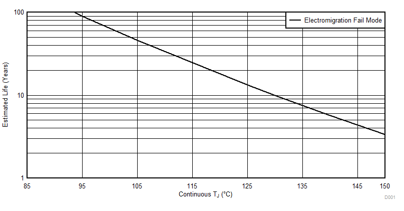
2. Silicon operating life design goal is 10 years at 105°C junction temperature (does not include package interconnect life).
Figure 1. CDCLVP111-SP Operating Life Derating Chart

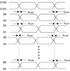
A. Output skew is calculated as the greater of: the difference between the fastest and the slowest tPLHn (n = 0, 1,...9) or the difference between the fastest and the slowest tPHLn (n = 0, 1,...9).
B. Part-to-part skew, is calculated as the greater of: The difference between the fastest and the slowest tPLHn (n = 0, 1,...9) across multiple devices or the difference between the fastest and the slowest tPHLn (n = 0, 1,...9) across multiple devices.
C. Typical value measured at ambient when clock input is 155.52 MHz for an integration bandwidth of 20 kHz to 5 MHz.
D. Input conditions: VCM = 1 V, VID = 0.5 V and FIN = 1 GHz.
Figure 2. Waveform for Calculating Both Output and Part-to-Part Skew

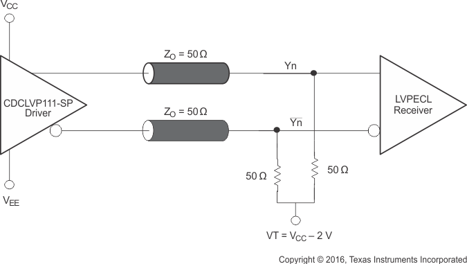
See Interfacing Between LVPECL, LVDS, and CML (SCAA056).
Figure 3. Typical Termination for Output Driver
6.8 Typical Characteristics

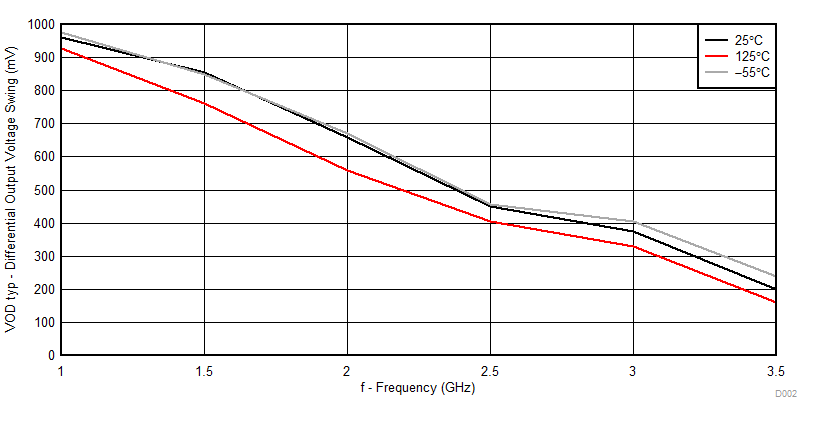
| Differential Output Voltage Swing vs Frequency | ||||
| VCC = 2.375 V | VCM = 1 V | VID = 0.5 V | ||