ZHCSFP6A November 2016 – January 2017 CDCLVP111-SP
PRODUCTION DATA.
8 Application and Implementation
NOTE
Information in the following applications sections is not part of the TI component specification, and TI does not warrant its accuracy or completeness. TI’s customers are responsible for determining suitability of components for their purposes. Customers should validate and test their design implementation to confirm system functionality.
8.1 Application Information
The CDCLVP111-SP is a low-additive jitter LVPECL fanout buffer that can generate 5 copies of 2 selectable LVDS, CML or SSTL inputs. The CDCLVP111-SP can accept reference clock frequencies up to 3.5 GHz while providing low-output skew.
8.2 Typical Application
8.2.1 Fanout Buffer for Line Card Application
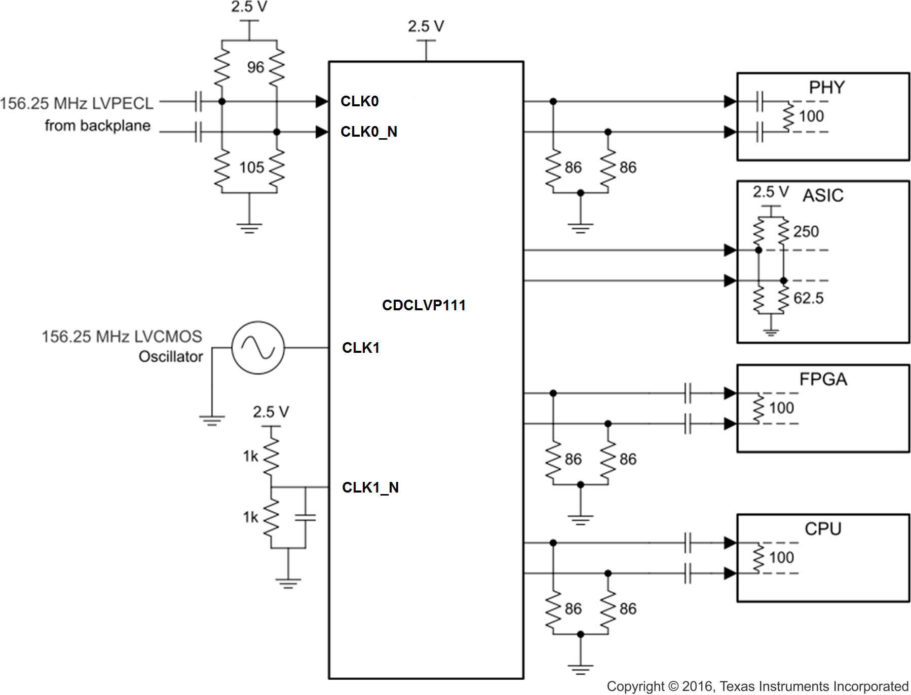 Figure 5. CDCLVP111-SP Block Diagram
8.2.1.1 Design Requirements
The CDCLVP111-SP shown in Figure 5 is configured to be able to select 2 inputs, a 156.25-MHz LVPECL clock from the backplane, or a secondary 156.25-MHz LVCMOS 2.5-V oscillator. Either signal can be then fanned out to desired devices, as shown.
The configuration example is driving 4 LVPECL receivers in a line card application with the following properties:
- The PHY device has internal AC coupling and appropriate termination and biasing. The CDCLVP111-SP will need to be provided with 86-Ω emitter resistors near the driver for proper operation.
- The ASIC is capable of DC coupling with a 2.5-V LVPECL driver such as the CDCLVP111-SP. This ASIC features internal termination so no additional components are needed.
- The FPGA requires external AC coupling but has internal termination. Again, 86-Ω emitter resistors are placed near the CDCLVP111-SP and a 0.1-uF are placed to provide AC coupling. Similarly, the CPU is internally terminated and requires external AC coupling capacitors.
8.2.1.2 Detailed Design Procedure
Unused outputs can be left floating.
In this example, the PHY, ASIC, and FPGA/CPU require different schemes. Power-supply filtering and bypassing is critical for low-noise applications.
See Figure 16 for recommended filtering techniques.
8.2.1.2.1 LVPECL Output Termination
Refer to Figure 6 for output termination schemes depending on the receiver application.
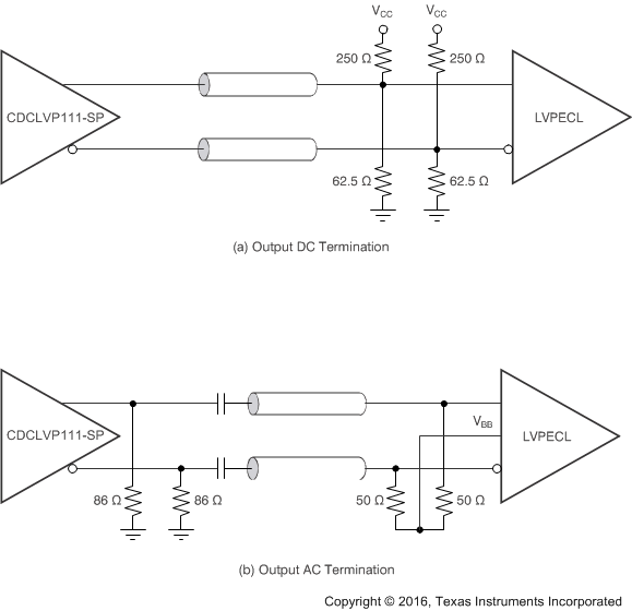 Figure 6. LVPECL Output DC and AC Termination for VCC = 2.5 V
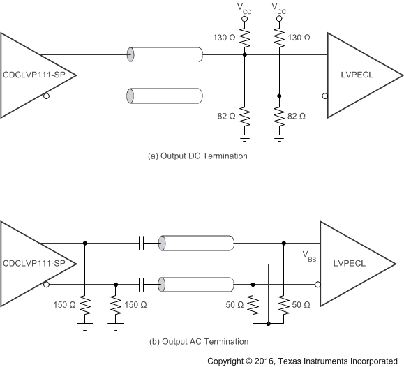 Figure 7. LVPECL Output DC and AC Termination for VCC = 3.3 V
8.2.1.2.2 Input Termination
The CDCLVP111-SP inputs can be interfaced with LVPECL, LVDS, or LVCMOS drivers. Figure 8 illustrates how to DC couple an LVCMOS input to the CDCLVP111-SP. The series resistance (RS) should be placed close to the LVCMOS driver; the value is calculated as the difference between the transmission line impedance and the driver output impedance.
Refer to Figure 8 for proper input terminations, dependent on single ended or differential inputs.
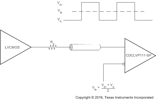 Figure 8. DC-Coupled LVCMOS Input to CDCLVP111-SP
Figure 9 shows how to DC couple LVDS inputs to the CDCLVP111-SP. Figure 10 and Figure 11 describe the method of DC coupling LVPECL inputs to the CDCLVP111-SP for VCC = 2.5 V and VCC = 3.3 V, respectively.
 Figure 9. DC-Coupled LVDS Inputs to CDCLVP111-SP
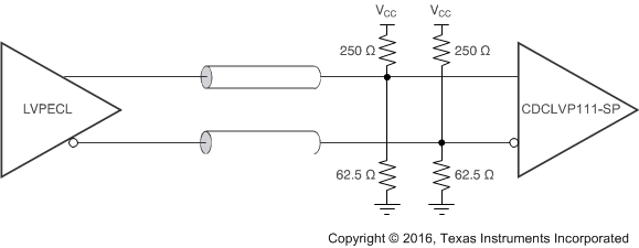 Figure 10. DC-Coupled LVPECL Inputs to CDCLVP111-SP (VCC = 2.5 V)
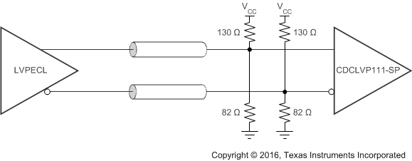 Figure 11. DC-Coupled LVPECL Inputs to CDCLVP111-SP (VCC = 3.3 V)
Figure 12 and Figure 13 show the technique of AC coupling differential inputs to the CDCLVP111-SP for VCC = 2.5 V and VCC = 3.3 V, respectively. TI recommends to place all resistive components close to either the driver end or the receiver end. If the supply voltages of the driver and receiver are different, AC coupling is required.
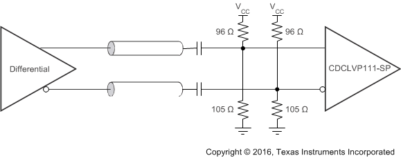 Figure 12. AC-Coupled Differential Inputs to CDCLVP111-SP (VCC = 2.5 V)
 Figure 13. AC-Coupled Differential Inputs to CDCLVP111-SP (VCC = 3.3 V)
8.2.1.3 Application Curves
The CDCLVP111-SP low-additive noise can be shown in this line card application. The low-noise, 110.22-MHz signal with 47-fs RMS jitter drives the CDCLVP111-SP, resulting in 192-fs RMS when integrated from 10 kHz to 20 MHz. The resultant-additive jitter is a low 186-fs RMS for this configuration.
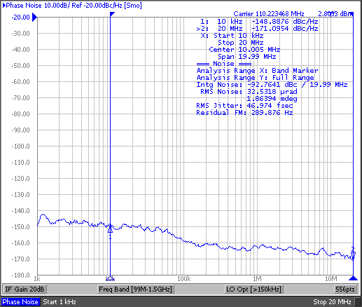
| Reference signal is low noise signal generator | ||
47-fs RMS
(10 kHz to 20 MHz)
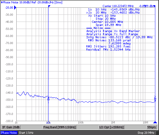
192-fs RMS
(10 kHz to 20 MHz)