SCAS881C August 2009 – January 2016 CDCLVP2102
PRODUCTION DATA.
- 1 Features
- 2 Applications
- 3 Description
- 4 Revision History
- 5 Pin Configuration and Functions
-
6 Specifications
- 6.1 Absolute Maximum Ratings
- 6.2 ESD Ratings
- 6.3 Recommended Operating Conditions
- 6.4 Thermal Information
- 6.5 Electrical Characteristics: LVCMOS Input, at VCC = 2.375 V to 3.6 V
- 6.6 Electrical Characteristics: Differential Input, at VCC = 2.375 V to 3.6 V
- 6.7 Electrical Characteristics: LVPECL Output, at VCC = 2.375 V to 2.625 V
- 6.8 Electrical Characteristics: LVPECL Output, at VCC = 3 V to 3.6 V
- 6.9 Timing Requirements, at VCC = 2.375 V to 2.625 V
- 6.10 Timing Requirements, at VCC = 3 V to 3.6 V
- 6.11 Typical Characteristics
- 7 Parameter Measurement Information
- 8 Detailed Description
- 9 Application and Implementation
- 10Power Supply Recommendations
- 11Layout
- 12Device and Documentation Support
- 13Mechanical, Packaging, and Orderable Information
6 Specifications
6.1 Absolute Maximum Ratings
over operating free-air temperature range (unless otherwise noted)(1)| MIN | MAX | UNIT | ||
|---|---|---|---|---|
| VCC | Supply voltage(2) | –0.5 | 4.6 | V |
| VIN | Input voltage(3) | –0.5 | VCC + 0.5 | V |
| VOUT | Output voltage(3) | –0.5 | VCC + 0.5 | V |
| IIN | Input current | 20 | mA | |
| IOUT | Output current | 50 | mA | |
| TA | Specified free-air temperature (no airflow) | –40 | 85 | °C |
| TJ | Maximum junction temperature | 125 | °C | |
| Tstg | Storage temperature | –65 | 150 | °C |
(1) Stresses beyond those listed under Absolute Maximum Ratings may cause permanent damage to the device. These are stress ratings only, which do not imply functional operation of the device at these or any other conditions beyond those indicated under Recommended Operating Conditions. Exposure to absolute-maximum-rated conditions for extended periods may affect device reliability.
(2) All supply voltages must be supplied simultaneously.
(3) The input and output negative voltage ratings may be exceeded if the input clamp-current and output clamp-current ratings are observed.
6.2 ESD Ratings
| VALUE | UNIT | |||
|---|---|---|---|---|
| V(ESD) | Electrostatic discharge | Human-body model (HBM), per ANSI/ESDA/JEDEC JS-001(1) | 2000 | V |
| Charged-device model (CDM), per JEDEC specification JESD22-C101(2) | 1500 | |||
(1) JEDEC document JEP155 states that 500-V HBM allows safe manufacturing with a standard ESD control process.
(2) JEDEC document JEP157 states that 250-V CDM allows safe manufacturing with a standard ESD control process.
6.3 Recommended Operating Conditions
over operating free-air temperature range (unless otherwise noted)| MIN | NOM | MAX | UNIT | |||
|---|---|---|---|---|---|---|
| VCC | Supply voltage | 2.375 | 2.5/3.3 | 3.60 | V | |
| TA | Ambient temperature | –40 | 85 | °C | ||
| TPCB | PCB temperature (measured at thermal pad) | 105 | °C | |||
6.4 Thermal Information
| THERMAL METRIC(1)(2)(3) | CDCLVP2102 | UNIT | ||
|---|---|---|---|---|
| RGT (VQFN) | ||||
| 16 PINS | ||||
| RθJA | Junction-to-ambient thermal resistance (0 LFM) | 51.8(4) | °C/W | |
| RθJC(top) | Junction-to-case (top) thermal resistance | 79 | °C/W | |
| RθJP(5) | Junction-to-pad thermal resistance | 6.12(4) | °C/W | |
| ψJT | Junction-to-top characterization parameter | 1.4 | °C/W | |
| ψJB | Junction-to-board characterization parameter | 19 | °C/W | |
| RθJC(bot) | Junction-to-case (bottom) thermal resistance | 6.12 | °C/W | |
(1) For more information about traditional and new thermal metrics, see the Semiconductor and IC Package Thermal Metrics application report (SPRA953).
(2) The package thermal resistance is calculated in accordance with JESD 51 and JEDEC 2S2P (high-K board).
(3) Connected to GND with four thermal vias (0.3-mm diameter).
(4) 2 × 2 vias on pad
(5) RθJP (junction-to-pad) is used for the VQFN package, because the primary heat flow is from the junction to the GND pad of the VQFN package.
6.5 Electrical Characteristics: LVCMOS Input, at VCC = 2.375 V to 3.6 V
at TA = –40°C to +85°C and TPCB ≤ 105°C (unless otherwise noted) (1)6.6 Electrical Characteristics: Differential Input, at VCC = 2.375 V to 3.6 V
at TA = –40°C to +85°C and TPCB ≤ 105°C (unless otherwise noted) (1)| PARAMETER | TEST CONDITIONS | MIN | TYP | MAX | UNIT | |
|---|---|---|---|---|---|---|
| fIN | Input frequency | Clock input | 2000 | MHz | ||
| VIN, DIFF, PP | Differential input peak-peak voltage | fIN ≤ 1.5 GHz | 0.1 | 1.5 | V | |
| 1.5 GHz ≤ fIN ≤ 2 GHz | 0.2 | 1.5 | V | |||
| VICM | Input common-mode level | 1 | VCC – 0.3 | V | ||
| IIH | Input high current | VCC = 3.6 V, VIH = 3.6 V | 40 | μA | ||
| IIL | Input low current | VCC = 3.6 V, VIL = 0 V | –40 | μA | ||
| ΔV/ΔT | Input edge rate | 20% to 80% | 1.5 | V/ns | ||
| ICAP | Input capacitance | 5 | pF | |||
6.7 Electrical Characteristics: LVPECL Output, at VCC = 2.375 V to 2.625 V
at TA = –40°C to +85°C and TPCB ≤ 105°C (unless otherwise noted) (1)| PARAMETER | TEST CONDITIONS | MIN | TYP | MAX | UNIT | |
|---|---|---|---|---|---|---|
| VOH | Output high voltage | TA = –40°C to 85°C | VCC – 1.26 | VCC – 0.9 | V | |
| TPCB ≤ 105°C | VCC – 1.26 | = | VCC – 0.83 | |||
| VOL | Output low voltage | TA = –40°C to 85°C | VCC – 1.7 | VCC – 1.3 | V | |
| TPCB ≤ 105°C | VCC – 1.7 | VCC – 1.25 | ||||
| VOUT, DIFF, PP | Differential output peak-peak voltage | fIN ≤ 2 GHz | 0.5 | 1.35 | V | |
| VAC_REF | Input bias voltage(2) | IAC_REF = 2 mA | VCC – 1.6 | VCC – 1.1 | V | |
| IEE | Supply internal current | Outputs unterminated, TA ≤ 85°C |
48 | mA | ||
| Outputs unterminated, TPCB ≤ 105°C |
49 | |||||
| ICC | Output and internal supply current | All outputs terminated, 50 Ω to VCC – 2 TA ≤ 85°C |
173 | mA | ||
| All outputs terminated, 50 Ω to VCC – 2 TPCB ≤ 105°C |
189 | |||||
6.8 Electrical Characteristics: LVPECL Output, at VCC = 3 V to 3.6 V
at TA = –40°C to +85°C and TPCB ≤ 105°C (unless otherwise noted)(1)(3) 100-MHz Wenzel oscillator, Input slew rate = 3.4 V/ns (differential)
(4) 122.88-MHz Rohde & Schwarz SMA100A, Input slew rate = 3.7 V/ns (differential)
(5) 156.25-MHz Crystek CPRO33 oscillator, Input slew rate = 2.9 V/ns (differential)
(6) 312.5-MHz Rohde & Schwarz SMA100A, Input slew rate = 4 V/ns (differential)
6.9 Timing Requirements, at VCC = 2.375 V to 2.625 V
Refer to Figure 1 and Figure 2.| MIN | NOM | MAX | UNIT | |||
|---|---|---|---|---|---|---|
| tPD | Propagation delay | VIN, DIFF, PP = 0.1 V | 450 | ps | ||
| VIN, DIFF, PP = 0.3 V | 450 | |||||
| tSK,PP | Part-to-part skew | 100 | ps | |||
| tSK,O_WB | Within bank output skew | 10 | ps | |||
| tSK,O_BB | Bank-to-bank output skew | Both inputs have equal skew | 15 | ps | ||
| tSK,P | Pulse skew (with 50% duty cycle input) | Crossing-point-to-crossing-point distortion, fOUT = 100 MHz | –50 | 50 | ps | |
| tRJIT | Random additive jitter (with 50% duty cycle input) | fOUT = 100 MHz, VIN,SE = VCC, Vth = 1.25 V, 10 kHz to 20 MHz |
0.089 | ps, RMS | ||
| fOUT = 100 MHz, VIN,SE = 0.9 V, Vth = 1.1 V, 10 kHz to 20 MHz |
0.093 | ps, RMS | ||||
| fOUT = 2 GHz, VIN,DIFF,PP = 0.2 V, VICM = 1 V, 10 kHz to 20 MHz |
0.037 | ps, RMS | ||||
| fOUT = 100 MHz, VIN,DIFF,PP = 0.15 V, VICM = 1 V, 10 kHz to 20 MHz |
0.094 | ps, RMS | ||||
| fOUT = 100 MHz, VIN,DIFF,PP = 1 V, VICM = 1 V, 10 kHz to 20 MHz |
0.091 | ps, RMS | ||||
| fOUT,8 = 500 MHz, VIN,DIFF,PP,0 = 0.15 V, VICM, 0 = 1 V, fOUT, 7 = 62.5 MHz, VIN,SE,1 = VCC, Vth, 1 = VCC/2 |
–52.5 | dBc | ||||
| PSPUR | Coupling on differential OUT8 from OUT7 in the frequency spectrum of fOUT, 8 ±(fOUT, 8/2) with synchronous inputs |
fOUT,8 = 500 MHz, VIN,DIFF,PP,0 = 0.15 V, VICM, 0 = 1 V, fOUT, 7 = 62.5 MHz, VIN,DIFF,PP,1 = 1 V, VICM, 1 = 1 V |
–66.8 | dBc | ||
| fOUT,8 = 500 MHz, VIN,DIFF,PP,0 = 0.15 V, VICM, 0 = 1 V, fOUT, 7 = 15.625 MHz, VIN,SE,1 = VCC, Vth, 1 = VCC/2 |
–52 | |||||
| fOUT,8 = 500 MHz, VIN,DIFF,PP,0 = 0.15 V, VICM, 0 = 1 V, fOUT, 7 = 15.625 MHz, VIN,DIFF,PP,1 = 1 V, VICM, 1 = 1 V |
–66.4 | |||||
| tR/tF | Output rise/fall time | 20% to 80% | 200 | ps | ||
6.10 Timing Requirements, at VCC = 3 V to 3.6 V
Refer to Figure 1 and Figure 2.| MIN | NOM | MAX | UNIT | |||
|---|---|---|---|---|---|---|
| tPD | Propagation delay | VIN, DIFF, PP = 0.1 V | 450 | ps | ||
| VIN, DIFF, PP = 0.3 V | 450 | |||||
| tSK,PP | Part-to-part skew | 100 | ps | |||
| tSK,O_WB | Within bank output skew | 10 | ps | |||
| tSK,O_BB | Bank-to-bank output skew | Both inputs have equal skew | 15 | ps | ||
| tSK,P | Pulse skew (with 50% duty cycle input) | Crossing-point-to-crossing-point distortion, fOUT = 100 MHz | –50 | 50 | ps | |
| tRJIT | Random additive jitter (with 50% duty cycle input) | fOUT = 100 MHz,(2) VIN,SE = VCC, Vth = 1.65 V, 10 kHz to 20 MHz |
0.081 | ps, RMS | ||
| fOUT = 100 MHz,(2) VIN,SE = 0.9 V, Vth = 1.1 V, 10 kHz to 20 MHz |
0.097 | ps, RMS | ||||
| fOUT = 2 GHz, VIN,DIFF,PP = 0.2 V, VICM = 1 V, 10 kHz to 20 MHz |
0.05 | ps, RMS | ||||
| fOUT = 100 MHz,(2) VIN,DIFF,PP = 0.15 V, VICM = 1 V, 10 kHz to 20 MHz |
0.098 | ps, RMS | ||||
| fOUT = 100 MHz,(2) VIN,DIFF,PP = 1 V, VICM = 1 V, 10 kHz to 20 MHz |
0.095 | ps, RMS | ||||
| fOUT,8 = 500 MHz, VIN,DIFF,PP,0 = 0.15 V, VICM, 0 = 1 V, fOUT, 7 = 62.5 MHz, VIN,SE,1 = VCC, Vth, 1 = VCC/2 |
–55.3 | dBc | ||||
| fOUT = 100 MHz(3), Input AC-coupled, VICM = VAC_REF, 12 kHz to 20 MHz |
0.068 | ps, RMS | ||||
| fOUT = 122.88 MHz(4), Input AC-coupled, VICM = VAC_REF, 12 kHz to 20 MHz |
0.056 | ps, RMS | ||||
| fOUT = 156.25 MHz(5), Input AC-coupled, VICM = VAC_REF, 12 kHz to 20 MHz |
0.047 | ps, RMS | ||||
| fOUT = 312.5 MHz(6), Input AC-coupled, VICM = VAC_REF, 12 kHz to 20 MHz |
0.026 | ps, RMS | ||||
| PSPUR | Coupling on differential OUT8 from OUT7 in the frequency spectrum of fOUT, 8 ±(fOUT, 8/2) with synchronous inputs |
fOUT,8 = 500 MHz, VIN,DIFF,PP,0 = 0.15 V, VICM, 0 = 1 V, fOUT, 7 = 62.5 MHz, VIN,SIFF,PP,1 = 1 V, VICM, 1 = 1 V |
–65.1 | dBc | ||
| fOUT,8 = 500 MHz, VIN,DIFF,PP,0 = 0.15 V, VICM, 0 = 1 V, fOUT, 7 = 15.625 MHz, VIN,SE,1 = VCC, Vth, 1 = VCC/2 |
–54.7 | |||||
| fOUT,8 = 500 MHz, VIN,DIFF,PP,0 = 0.15 V, VICM, 0 = 1 V, fOUT, 7 = 15.625 MHz, VIN,DIFF,PP,1 = 1 V, VICM, 1 = 1 V |
–66.7 | |||||
| tR/tF | Output rise/fall time | 20% to 80% | 200 | ps | ||
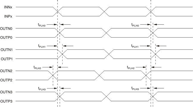
Figure 1 shows the output voltage and rise/fall time. Output and part-to-part skew are shown in Figure 2.
 Figure 1. Output Voltage and Rise/Fall Time

1. Output skew is calculated as the greater of the following: As the difference between the fastest and the slowest tPLHn (n = 0, 1, 2, 3), or as the difference between the fastest and the slowest tPHLn (n = 0, 1, 2, 3).
2. Part-to-part skew is calculated as the greater of the following: As the difference between the fastest and the slowest tPLHn (n = 0, 1, 2, 3) across multiple devices, or the difference between the fastest and the slowest tPHLn (n = 0, 1, 2, 3) across multiple devices.
Figure 2. Output and Part-to-Part Skew
6.11 Typical Characteristics
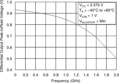
at TA = –40°C to +85°C (unless otherwise noted) Figure 3. Differential Output Peak-to-Peak Voltage vs Frequency
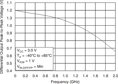
 Figure 4. Differential Output Peak-to-Peak Voltage vs Frequency