ZHCSF03 March 2016 CDCM6208V2G
PRODUCTION DATA.
- 1 特性
- 2 应用
- 3 说明
- 4 简化电路原理图
- 5 修订历史记录
- 6 说明 (续)
- 7 Pin Configuration and Functions
-
8 Specifications
- 8.1 Absolute Maximum Ratings
- 8.2 ESD Ratings
- 8.3 Recommended Operating Conditions
- 8.4 Thermal Information, Airflow = 0 LFM
- 8.5 Thermal Information, Airflow = 150 LFM
- 8.6 Thermal Information, Airflow = 250 LFM
- 8.7 Thermal Information, Airflow = 500 LFM
- 8.8 Single Ended Input Characteristics
- 8.9 Single Ended Input Characteristics (PRI_REF, SEC_REF)
- 8.10 Differential Input Characteristics (PRI_REF, SEC_REF)
- 8.11 Crystal Input Characteristics (SEC_REF)
- 8.12 Single Ended Output Characteristics (STATUS1, STATUS0, SDO, SDA)
- 8.13 PLL Characteristics
- 8.14 LVCMOS Output Characteristics
- 8.15 LVPECL (High-Swing CML) Output Characteristics
- 8.16 CML Output Characteristics
- 8.17 LVDS (Low-Power CML) Output Characteristics
- 8.18 HCSL Output Characteristics
- 8.19 Output Skew and Sync to Output Propagation Delay Characteristics
- 8.20 Device Individual Block Current Consumption
- 8.21 Worst Case Current Consumption
- 8.22 I2C TIMING
- 8.23 SPI Timing Requirements
- 8.24 Typical Characteristics
- 9 Parameter Measurement Information
- 10Detailed Description
-
11Application and Implementation
- 11.1 Application Information
- 11.2
Typical Applications
- 11.2.1
Design Requirements
- 11.2.1.1 Device Block-level Description
- 11.2.1.2 Device Configuration Control
- 11.2.1.3 Configuring the RESETN Pin
- 11.2.1.4 Preventing False Output Frequencies in SPI/I2C Mode at Startup:
- 11.2.1.5 Power Down
- 11.2.1.6 Device Power Up Timing:
- 11.2.1.7 Input Mux and Smart Input Mux
- 11.2.1.8 Universal INPUT Buffer (PRI_REF, SEC_REF)
- 11.2.1.9 VCO Calibration
- 11.2.1.10 Reference Divider (R)
- 11.2.1.11 Input Divider (M)
- 11.2.1.12 Feedback Divider (N)
- 11.2.1.13 Prescaler Dividers (PS_A, PS_B)
- 11.2.1.14 Phase Frequency Detector (PFD)
- 11.2.1.15 Charge Pump (CP)
- 11.2.1.16
Programmable Loop Filter
- 11.2.1.16.1 Loop Filter Component Selection
- 11.2.1.16.2 Device Output Signaling
- 11.2.1.16.3 Integer Output Divider (IO)
- 11.2.1.16.4 Fractional Output Divider (FOD)
- 11.2.1.16.5 Output Synchronization
- 11.2.1.16.6 Output MUX on Y4 and Y5
- 11.2.1.16.7 Staggered CLK Output Powerup for Power Sequencing of a DSP
- 11.2.2 Detailed Design Procedure
- 11.2.3 Application Performance Plots
- 11.2.1
Design Requirements
- 12Power Supply Recommendations
- 13Layout
- 14器件和文档支持
- 15机械、封装和可订购信息
11 Application and Implementation
NOTE
Information in the following applications sections is not part of the TI component specification, and TI does not warrant its accuracy or completeness. TI’s customers are responsible for determining suitability of components for their purposes. Customers should validate and test their design implementation to confirm system functionality.
11.1 Application Information
The CDCM6208 is a highly integrated clock generator and jitter cleaner. The CDCM6208 derives its output clocks from an on-chip oscillator which can be buffered through integer or fractional output dividers.
11.2 Typical Applications
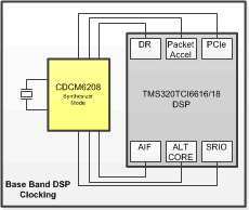 Figure 36. Typical Application Circuit
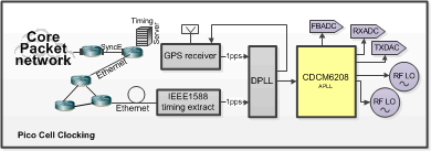 Figure 37. Typical Application Circuit
11.2.1 Design Requirements
The most jitter sensitive application besides driving A-to-D converters are systems deploying a serial link using Serializer and De-serializer implementation (for example, a 10 GigEthernet). Fully estimating the clock jitter impact on the link budget requires an understanding of the transmit PLL bandwidth and the receiver CDR bandwidth.
11.2.1.1 Device Block-level Description
The CDCM6208V2G includes an on-chip PLL with an on-chip VCO. The PLL blocks consist of a universal input interface, a phase frequency detector (PFD), charge pump, partially integrated loop filter, and a feedback divider. Completing the CDCM6208V2G device are the combination of integer and fractional output dividers, and universal output buffers. The PLL is powered by on-chip low dropout (LDO), linear voltage regulators and the regulated supply network is partitioned such that the sensitive analog supplies are running from separate LDOs than the digital supplies which use their own LDO. The LDOs provide isolation of the PLL from any noise in the external power supply rail with a PSNR of better than -50 dB at all frequencies. The regulator capacitor pin REG_CAP should be connected to ground by a 10 µF capacitor with low ESR (e.g. below 1 Ω ESR) to ensure stability.
11.2.1.2 Device Configuration Control
Figure 39 illustrates the relationships between device states, the control pins, device initialization and configuration, and device operational modes. In pin mode, the state of the control pins determines the configuration of the device for all device states. In programming mode, the device registers are initialized to their default state and the host can update the configuration by writing to the device registers. A system may transition a device from pin mode to host connected mode by changing the state of the SI_MODE pins and then triggering a device reset (either via the RESETN pin or via setting the RESETN bit in the device registers). In reset, the device disables the outputs so that unwanted sporadic activity associated with device initialization does not appear on the device outputs.
11.2.1.3 Configuring the RESETN Pin
Figure 38 shows two typical applications examples of the RESETN pin.
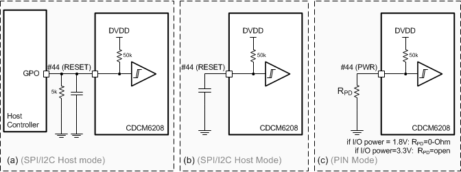 Figure 38. RESETN/PWR Pin Configurations
Figure 38 (a) SPI / I2C mode only: shows the RESETN pin connected to a digital device that controls device reset. The resistor and capacitor combination ensure reset is held low even if the CDCM6208V2G is powered up before the host controller output signal is valid.
Figure 38 (b) SPI / I2C mode only:shows a configuration in which the user wishes to introduce a delay between the time that the system applies power to the device and the device exiting reset. If the user does not use a capacitor, then the device effectively ignores the state of the RESETN pin.
Figure 38 (c) Pin mode only: shows a configuration useful if the device is used in Pin Mode. Here device pin number 44 becomes the PWR input. An external pull down resistor can be used to pull this pin down. If the resistor is not installed, the pin is internally pulled high.
Figure 39 shows how the different possible device configurations and when the VCO becomes calibrated and the outputs turn on and off.
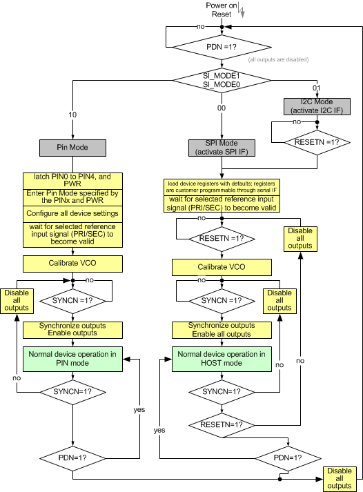 Figure 39. Device Power up and Configuration
11.2.1.4 Preventing False Output Frequencies in SPI/I2C Mode at Startup:
Some systems require a custom configuration and cannot tolerate any output to start up with a wrong frequency. Holding RESET low at power-up until the device is fully configured keeps all outputs disabled. The device calibrates automatically after RESET becomes released and starts out with the desired output frequency.
NOTE
The RESETN pin cannot be held low during I2C communication. Instead, use the SYNC pin to disable the outputs during an I2C write operation, and toggle RESETN pin afterwards. Alternatively, other options exist such as using the RESETN bit in the register space to disable outputs until the write operation is complete.
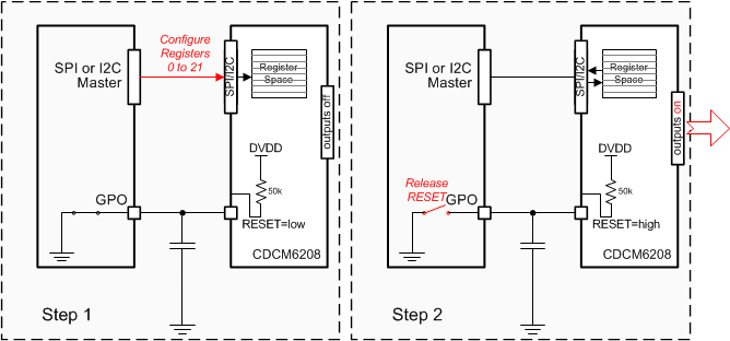 Figure 40. Reset Pin Control During Register Loading
11.2.1.5 Power Down
When the PDN pin = 0, the device enters a complete power down mode with a current consumption of no more than 1 mA from the entire device.
11.2.1.6 Device Power Up Timing:
Before the device outputs turn on after power up, the device goes through the following initialization routine:
Table 34. Initialization Routine
| STEP | DURATION | COMMENTS |
|---|---|---|
| Step 1: Power up ramp | Depends on customer supply ramp time | The POR monitor holds the device in power-down or reset until the VDD supply voltage reaches 1.06 V (min) to 1.26 V (max) |
| Step 2: XO startup (if crystal is used) | Depends on XTAL. Could be several ms; For NX3225GA 25 MHz typical XTAL startup time measures 200 µs. |
This step assumes RESETN = 1 and PDN = 1.The XTAL startup time is the time it takes for the XTAL to oscillate with sufficient amplitude. The CDCM6208V2G has a built-in amplitude detection circuit, and holds the device in reset until the XTAL stage has sufficient swing. |
| Step 3: Ref Clock Counter | 64k Reference clock cycles at PFD input | This counter of 64 k clock cycles needs to expire before any further power-up step is done inside the device. This counter ensures that the input to the PFD from PRI or SEC input has stabilized in frequency. The duration of this step can range from 640 µs (fPFD= 100 MHz) to 8 sec (8 kHz PFD). |
| Step 4: FBCLK counter | 64k FBCLK cycles with CW=32; The duration is similar to Step 3, or can be more accurately estimated as: Approximately 64k x PS_A x N/2.48 GHz |
The Feedback counter delays the startup by another 64k PFD clock cycles. This is so that all counters are well initialized and also ensure additional timing margin for the reference clock to settle. This step can range from 640 µs (fPFD= 100 MHz) to 8 sec (fPFD= 8kHz). |
| Step 5: VCO calibration | 128k PFD reference clock cycles | This step calibrates the VCO to the exact frequency range, and takes exactly 128k PFD clock cycles. The duration can therefore range from 1280 µs (fPFD= 100 MHz) to 16 sec (f PFD= 8 KHz). |
| Step 6: PLL lock time | approximately 3 x LBW | The Outputs turn on immediately after calibration. A small frequency error remains for the duration of approximately 3 x LBW (so in synthesizer mode typically 10 µs). The initial output frequency will be lower than the target output frequency, as the loop filter starts out initially discharged. |
| Step 7: PLL Lock indicator high | approximately 2305 PFD clock cycles | The PLL lock indicator if selected on output STATUS0 or STATUS1 will go high after approximately 2048 to 2560 PFD clock cycles to indicate PLL is now locked. |
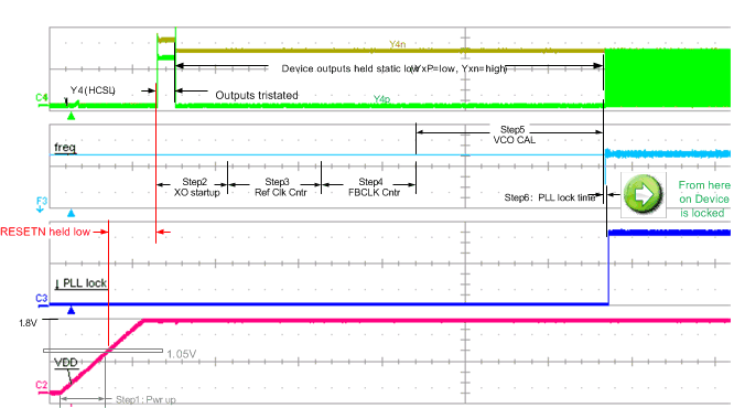 Figure 41. Powerup Time
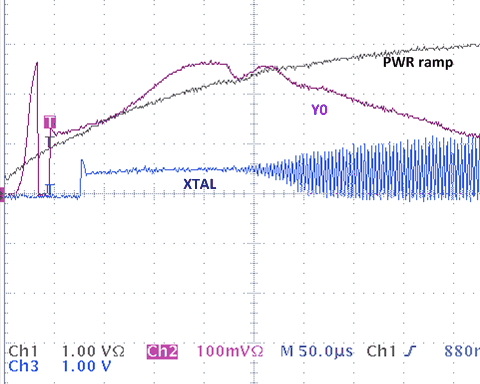 Figure 42. XTAL Startup Using NX3225GA 25 MHz (Step 2)
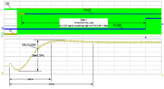 Figure 43. PLL Lock Behavior (Step 6)
11.2.1.7 Input Mux and Smart Input Mux
The Smart Input MUX supports auto-switching and manual-switching using control pin (and through register). The Smart Input MUX is designed such that glitches created during switching in both auto and manual modes are suppressed at the MUX output.
Table 35. Input Mux Selection
| SI_MODE1 PIN NO. 47 |
REGISTER 4 BIT 13SMUX_MODE_SEL | REGISTER 4 BIT 12 SMUX_REF_SEL | REF_SEL PIN NO. 6 |
SELECTED INPUT | |
|---|---|---|---|---|---|
| 0 (SPI/I2C mode) | 0 | X | X | Auto Select Priority is given to Primary Reference input. | |
| 1 | 0 | 1 | Primary input | input select through SPI/I2C | |
| 1 | Secondary input | ||||
| 1 | 0 | Primary input | input select through external pin | ||
| 1 | Secondary input | ||||
| 1 (pin mode) | not available | 0 | Primary or Auto (see Table 4) | ||
| 1 | Secondary or Auto (see Table 4) | ||||
Example 1:An application desired to auto-select the clock reference in SPI/I2C mode. During production testing however, the system needs to force the device to use the primary followed by the secondary input. The settings would be as follows:
- Tie REF_SEL pin always high
- For primary clock input testing, use R4[13:12] = 10
- For secondary clock input testing, set R4[13:12] = 11.
- For the auto-mux setting in the final product shipment, set R3[13:12]=01 or 00
Example 2: The application wants to select the clock input manually without programming SPI/I2C. In this case, program R4[13:12] = 11, and select primary or secondary input by toggling REF_SEL low or high.
SmartMux input frequency limitation: In the automatic mode, the frequencies of both inputs to the smart mux (PRI_REF divided by R and SEC_REF) need to be similar; however, they can vary by up to 20%.
Switching behavior: The input clocks can have any phase. When switching happens between one input clock to the other, the phase of the output clock slowly transitions to the phase of the newly selected input clock. There will be no-phase jump at the output. The phase transition time to the new reference clock signal depends on the PLL loop filter bandwidth. Auto-switch assigns higher priority to PRI_REF and lower priority to SEC_REF. The timing diagram of an auto-switch at the input MUX is shown in Figure 44.
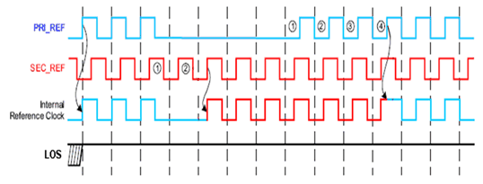 Figure 44. Smart Input MUX Auto-Switch Mode Timing Diagram
11.2.1.8 Universal INPUT Buffer (PRI_REF, SEC_REF)
The universal input buffers support multiple signaling formats (LVDS, CML or LVCMOS) and these require external termination schemes. The secondary input buffer also supports crystal inputs and Table 28 provides the characteristics of the crystal that can be used. Both inputs incorporate hysteresis.
11.2.1.9 VCO Calibration
The LC VCO is designed using high-Q monolithic inductors and has low phase noise characteristics. The VCO of the CDCM6208V2G must be calibrated to ensure that the clock outputs deliver optimal phase noise performance. Fundamentally, a VCO calibration establishes an optimal operating point within the tuning range of the VCO. While transparent to the user, the CDCM6208V2G and the host system perform the following steps comprising a VCO calibration sequence:
- Normal Operation- When the CDCM6208V2G is in normal (operational) mode, the state of both the power down pin (PDN) and reset pin (RESETN) is high.
- Entering the reset state – If the user wishes to restore all device defaults and initiate a VCO calibration sequence, then the host system must place the device in reset via the PDN pin, via the RESETN pin, or by removing and restoring device power. Pulling either of these pins low places the device in the reset state. Holding either pin low holds the device in reset.
- Exiting the reset state – The device calibrates the VCO either by exiting the device reset state or through the device reset command initiated via the host interface. Exiting the reset state occurs automatically after power is applied and/or the system restores the state of the PDN or RESETN pins from the low to high state. Exiting the reset state using this method causes the device defaults to be loaded/reloaded into the device register bank. Invoking a device reset via the register bit does not restore device defaults; rather, the device retains settings related to the current clock frequency plan. Using this method allows for a VCO calibration for a frequency plan other than the default state (i.e. the device calibrates the VCO based on the settings contained within the register bank at the time that the register bit is accessed). The nominal state of this bit is low. Writing this bit to a high state and then returning it to the low state invokes a device reset without restoring device defaults.
- Device stabilization – After exiting the reset state as described in Step 3, the device monitors internal voltages and starts a reset timer. Only after internal voltages are at the correct level and the reset time has expired will the device initiate a VCO calibration. This ensures that the device power supplies and phase locked loops have stabilized prior to calibrating the VCO.
- VCO Calibration – The CDCM6208V2G calibrates the VCO. During the calibration routine, the device holds all outputs in reset so that the CDCM6208V2G generates no spurious clock signals.
11.2.1.10 Reference Divider (R)
The reference (R) divider is a continuous 4-b counter (1 – 16) that is present on the primary input before the Smart Input MUX. It is operational in the frequency range of 8 kHz to 250 MHz. The output of the R divider sets the input frequency for the Smart MUX, and the auto switch capability of the Smart MUX can then be employed as long as the secondary input frequency is no more than ± 20% different from the output of the R divider.
11.2.1.11 Input Divider (M)
The input (M) divider is a continuous 14-b counter (1 – 16384) that is present after the Smart Input MUX. It is operational in the frequency range of 8 kHz to 250 MHz. The output of the M divider sets the PFD frequency to the PLL and should be in the range of 8 kHz to 100 MHz.
11.2.1.12 Feedback Divider (N)
The feedback (N) divider is made up of cascaded 8-b counter divider (1 – 256) followed by a 10-b counter divider (1 – 1024) that are present on the feedback path of the PLL. It is operational in the frequency range of 8 kHz to 800 MHz. The output of the N divider sets the PFD frequency to the PLL and should be in the range of 8 kHz to 100 MHz. The frequency out of the first divider is required to be less than or equal to 200 MHz to ensure proper operation.
11.2.1.13 Prescaler Dividers (PS_A, PS_B)
The prescaler (PS) dividers are fed by the output of the VCO and are distributed to the output dividers (PS_A to the dividers for Outputs 0, 1, 4, and 5 and PS_B to the dividers for Outputs 2, 3, 6, and 7. PS_A also completes the PLL as it also drives the input of the Feedback Divider (N).
11.2.1.14 Phase Frequency Detector (PFD)
The PFD takes inputs from the Smart Input MUX output and the feedback divider output and produces an output that is dependent on the phase and frequency difference between the two inputs. The allowable range of frequencies at the inputs of the PFD is from 8 kHz to 100 MHz.
11.2.1.15 Charge Pump (CP)
The charge pump is controlled by the PFD which dictates either to pump up or down in order to charge or discharge the integrating section of the on-chip loop filter. The integrated and filtered charge pump current is then converted to a voltage that drives the control voltage node of the internal VCO through the loop filter. The range of the charge pump current is from 500 µA to 4 mA.
11.2.1.16 Programmable Loop Filter
The on-chip PLL supports a partially internal and partially external loop filter configuration for all PLL loop bandwidths where the passive external components C1, C2, and R2 are connected to the ELF pin as shown in Figure 45 to achieve PLL loop bandwidths from 400 kHz down to 10 Hz.
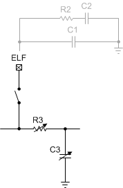 Figure 45. CDCM6208V2G PLL Loop Filter Topology
11.2.1.16.1 Loop Filter Component Selection
The loop filter setting and external resistor selection is important to set the PLL to best possible bandwidth and to minimize jitter. A high bandwidth (≥ 100 kHz) provides best input signal tracking and is therefore desired with a clean input reference (synthesizer mode). A low bandwidth (≤ 1 kHz) is desired if the input signal quality is unknown (jitter cleaner mode). TI provides a software tool that makes it easy to select the right loop filter components. C1, R2, and C2 are external loop filter components, connected to the ELF pin. The 3 rd pole of the loop filter is device internal with R3 and C3 register selectable.
11.2.1.16.2 Device Output Signaling
LVDS-like: All outputs Y[7:0] support LVDS-like signaling. The actual output stage uses a CML structure and drives a signal swing identical to LVDS (~350mV). The output slew rate is faster than standard LVDS for best jitter performance. The LVDS-like outputs should be AC-coupled when interfacing to a LVDS receiver. See reference schematic Figure 63 for an example. The supply voltage for outputs configured LVDS can be selected freely between 1.8 V and 3.3 V.
LVPECL-like: Outputs Y[3:0] support LVPECL-like signaling. The actual output stage uses a CML structure but drives the same signal amplitude and rise time as true emitter coupled logic output stages. The LVPECL-like outputs should be AC-coupled, and contrary to standard PECL designs, no external termination resistor to VCC-2V is used (fewer components for lowest BOM cost). See reference schematic Figure 63 for an example. The supply voltage for outputs configured LVPECL-like is recommended to be 3.3 V, though even 1.8 V provides nearly the same output swing and performance at much lower power consumption.
CML: Outputs Y[3:0] support standard CML signaling. The supply voltage for outputs configured CML can be selected freely between 1.8 V and 3.3 V. A true CML receiver can be driven DC coupled. All other differential receiver should connected using AC coupling. See reference schematic Figure 63 for a circuit example.
HCSL: Outputs Y[7:4] support HCSL signaling. The supply voltage for outputs configured HCSL can be selected freely between 1.8 V and 3.3 V. HCSL is referenced to GND, and requires external 50 Ω termination to GND. See reference schematic for an example.
CMOS: Outputs Y[7:4] support 1.8 V, 2.5 V, and 3.3 V CMOS signaling. A fast or reduced slew rate can be selected through register programming. Each differential output port can drive one or two CMOS output signals. Both signals are “in-phase”, meaning their phase offset is zero degrees, and not 180˚. The output swing is set by providing the according supply voltage (for example, if VDD_Y4=2.5 V, the output swing on Y4 will be 2.5 V CMOS). Outputs configured for CMOS should only be terminated with a series-resistor near the device output to preserve the full signal swing. Terminating CMOS signals with a 50 Ω resistor to GND would reduce the output signal swing significantly.
11.2.1.16.3 Integer Output Divider (IO)
Each integer output divider is made up of a continuous 10-b counter. The output buffer itself contributes only little to the total device output jitter due to a low output buffer phase noise floor. The typical output phase noise floor at an output frequency of 122.88 MHz, 20 MHz offset from the carrier measures as follows: LVCMOS: -157.8 dBc/Hz, LVDS: -158 dBc/Hz, LVPECL: -158.25 dBc/Hz, HCSL: -160 dBc/Hz. Therefore, the overall contribution of the output buffer to the total jitter is approximately 50 fs-rms (12 k - 20 MHz). An actual measurement of phase noise floor with different output frequencies for one nominal until yielded the following:
Table 36. Integer Output Divider (IO)
| fOUT | LVDS (Y0) | PECL (Y0) | CML (Y0) | HCSL (Y4) | CMOS 3p3V (Y7) |
|---|---|---|---|---|---|
| 737.28 MHz | -154.0 dBc/Hz | -154.8 dBc/Hz | -154.4 dBc/Hz | -153.1 dBc/Hz | -150.9 dBc/Hz |
| 368.64 MHz | -157.0 dBc/Hz | -155.8 dBc/Hz | -156.4 dBc/Hz | -153.9 dBc/Hz | -153.1 dBc/Hz |
| 184.32 MHz | -157.3 dBc/Hz | -158.6 dBc/Hz | 158.1 dBc/Hz | -154.7 dBc/Hz | -156.2 dBc/Hz |
| 92.16 MHz | -161.2 dBc/Hz | -161.6 dBc/Hz | -161.4 dBc/Hz | -155.2 dBc/Hz | -159.4 dBc/Hz |
| 46.08 MHz | -162.2 dBc/Hz | -165.0 dBc/Hz | -163.0 dBc/Hz | -154.0 dBc/Hz | -162.8 dBc/Hz |
11.2.1.16.4 Fractional Output Divider (FOD)
The CDCM6208V2G incorporates a fractional output divider on Y[7:4], allowing these outputs to run at non-integer output divide ratios of the PLL frequencies. This feature is useful when systems require different, unrelated frequencies. The fractional output divider architecture is shown in Figure 46.
 Figure 46. Fractional Output Divider Principle Architecture
(Simplified Graphic, not Showing Output Divider Bypass Options)
The fractional output divider requires an input frequency between 400 MHz and 800 MHz, and outputs any frequency equal or less than 400 MHz (the minimum fractional output divider setting is 2). The fractional divider block has a first stage integer pre-divider followed by a fractional sigma-delta output divider block that is deep enough such as to generate any output frequency in the range of 0.78 MHz to 400 MHz from any input frequency in the range of 400 MHz to 800 MHz with a worst case frequency accuracy of no more than ±1ppm. The fractional values available are all possible 20-b representations of fractions within the following range:
- 1.0 ≤ ƒracDIV ≤ 1.9375
- 2.0 ≤ ƒracDIV ≤ 3.875
- 4.0 ≤ ƒracDIV ≤ 5.875
- x.0 ≤ ƒracDIV ≤ (x + 1) + 0.875 with x being all even numbers from x = 2, 4, 6, 8, 10, ...., 254
- 254.0 ≤ ƒracDIV ≤ 255.875
- 256.0 ≤ ƒracDIV ≤ 256.99999
The CDCM6208V2G user GUI comprehends the fractional divider limitations; therefore, using the GUI to comprehend frequency planning is recommended.
The fractional divider output jitter is a function of fractional divider input frequency and furthermore depends on which bits are exercised within the fractional divider. Exercising only MSB or LSB bits provides better jitter than exercising bits near the center of the fractional divider. Jitter data are provided in this document, and vary from 50 ps-pp to 200 ps-pp, when the device is operated as a frequency synthesizer with high PLL bandwidths (approximately 100 kHz to 400 kHz). When the device is operated as a jitter cleaner with low PLL bandwidths (< 1 kHz), its additive total jitter increases by as much as 30 ps-pp. The fractional divider can be used in integer mode. However, if only an integer divide ratio is needed, it is important to disable the corresponding fractional divider enable bit, which engages the higher performing integer divider.
11.2.1.16.5 Output Synchronization
Both types of output dividers can be synchronized using the SYNCN signal. For the CDCM6208V2G, this signal comes from the SYNCN pin or the soft SYNCN register bit R3.5. The most common way to execute the output synchronization is to toggle the SYNCN pin. When SYNC is asserted (VSYNCN ≤ VIL), all outputs are disabled (high-impedance) and the output dividers are reset. When SYNC is de-asserted (VSYNCN ≥ VIH), the device first internally latches the signal, then retimes the signal with the pre-scaler, and finally turns all outputs on simultaneously. The first rising edge of the outputs is therefore approximately 15 ns to 20 ns delayed from the SYNC pin assertion. For one particular device configuration, the uncertainty of the delay is ±1 PS_A clock cycles. For one particular device and one particular configuration, the delay uncertainty is one PS_A clock cycle.
The SYNC feature is particularly helpful in systems with multiple CDCM6208V2G. If SYNC is released simultaneously for all devices, the total remaining output skew uncertainty is ±1 clock cycles for all devices configured to identical pre-scaler settings. For devices with varying pre-scaler settings, the total part-to-part skew uncertainty due to sync remains ±2 clock cycles.
Outputs Y0, Y1, Y4, and Y5 are aligned with the PS_A output while outputs Y2, Y3, Y6, and Y7 are aligned with the PS_B output). All outputs Y[7:0] turn on simultaneously, if PS_B and PS_A are set to identical divide values (PS_A=PS_B).
 Figure 47. SYNCN to Output Delay Uncertainty
11.2.1.16.6 Output MUX on Y4 and Y5
The CDCM6208V2G device outputs Y4 and Y5 can either be used as independent fractional outputs or allow bypassing of the PLL in order to output the primary or secondary input signal directly.
11.2.1.16.7 Staggered CLK Output Powerup for Power Sequencing of a DSP
DSPs are sensitive to any kind of voltage swing on unpowered input rails. To protect the DSP from long-term reliability problems, it is recommended to avoid any clock signal to the DSP until the DSP power rail is also powered up. This can be achieved in two ways using the CDCM6208V2G:
- Digital control: Initiating a configuration of all registers so that all outputs are disabled, and then turning on outputs one by one through serial interface after each DSP rail becomes powered up accordingly.
- Output Power supply domain control: An even easier scheme might be to connect the clock output power supply VDD_Yx to the corresponding DSP input clock supply domain. In this case, the CDCM6208V2G output will remain disabled until the DSP rails ramps up as well. Figure 48 shows the turn-on behavior.
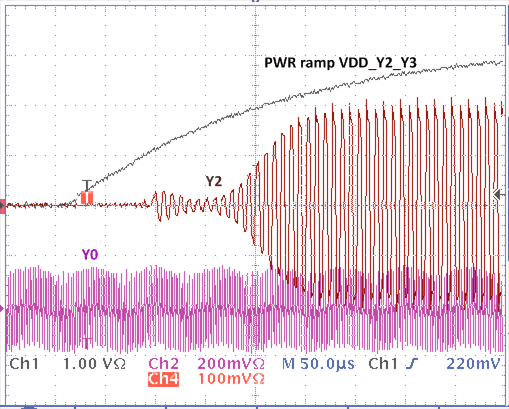 Figure 48. Sequencing the Output Turn-on Through Sequencing the Output Supplies. Output Y2 Powers Up While Output Y0 is Already Running.
11.2.2 Detailed Design Procedure
11.2.2.1 Jitter Considerations in SERDES Systems
The most jitter sensitive application besides driving A-to-D converters are systems deploying a serial link using Serializer and De-serializer implementation (for example, 10 GigEthernet). Fully estimating the clock jitter impact on the link budget requires an understanding of the transmit PLL bandwidth and the receiver CDR bandwidth. As can be seen in Figure 49, the bandwidth of TX and RX is the frequency range in which clock jitter adds without any attenuation to the jitter budget of the link. Outside of these frequencies, the SERDES link will attenuate clock jitter with a 20 dB/dec or even steeper roll-off.
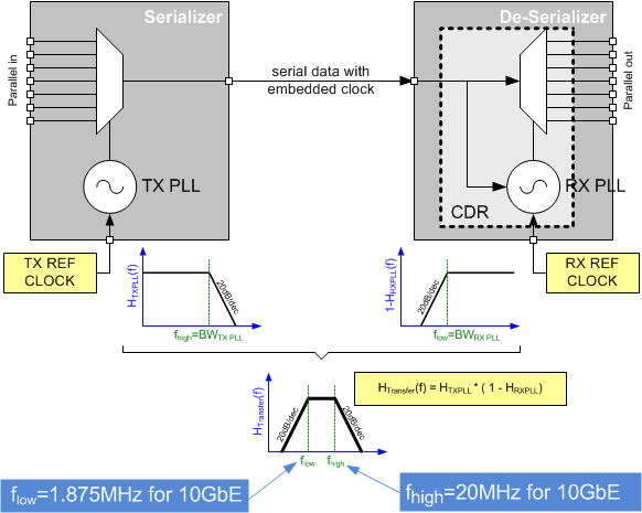 Figure 49. Serial Link Jitter Budget Explanation
Example: SERDES link with KeyStone™ I DSP
The SERDES TX PLL of the TI KeyStone™ I DSP family (see SPRABI2) for the SRIO interface, has a 13 MHz PLL bandwidth (Low Pass Characteristic, see Figure 49). The CDCM6208V2, pin-mode 27, was characterized in this example over Process, Voltage and Temperature (PVT) with a low pass filter of 13 MHz to simulate the TX PLL. The attenuation is higher or equal to 20 dB/dec; therefore, the characterization used 20 dB/dec as worst case.
Table 37 shows the maximum Total Jitter(1) over PVT with and without Low Pass Filter.
Table 37. Maximum Total Jitter Over PVT With and Without Low Pass Filter
| OUTPUT | FREQUENCY [MHz] |
MAX TJ [ps] DSP SPEC |
MAX TJ [ps] without LOW PASS FILTER |
MAX TJ [ps] with 13 MHz LOW PASS FILTER |
|---|---|---|---|---|
| Y0 | 122.88 | 56 | 9.43 | 8.19 |
| Y2 | 30.72 | 56 | 9.60 | 7.36 |
| Y3 | 30.72 | 56 | 9.47 | 7.42 |
| Y4 | 156.25 (6 bit fraction) |
56 | 57.66 | 17.48 |
| Y5 | 156.25 (20 bit fraction) |
56 | 76.87 | 32.32 |
| Y6 | 100.00 | 56 | 86.30 | 33.86 |
| Y7 | 66.667 | 300 | 81.71 | 35.77 |
Figure 50 shows the maximum Total Jitter with, without Low Pass Filter characteristic and the maximum TI KeyStone™ I specification.
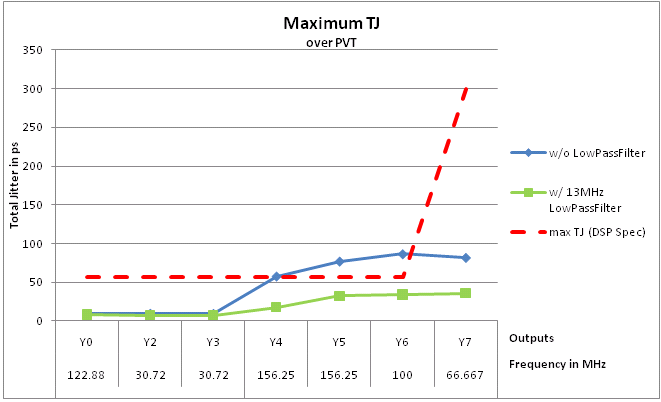 Figure 50. Maximum Jitter Over PVT
NOTE
Due to the damping characteristic of the DSP SERDES PLLs, the actual TJ data can be worse.
11.2.2.2 Jitter Considerations in ADC and DAC Systems
A/D and D/A converters are sensitive to clock jitter in two ways: They are sensitive to phase noise in a particular frequency band, and also have maximum spur level requirements to achieve maximum noise floor sensitivity. The following test results were achieved connecting the CDCM6208V2G to ADC and DACs:
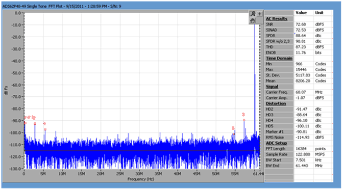 Figure 51. IF = 60 MHz Fclk = 122.88 MHz Baseline (Lab Clk Generator) ADC: ADS62P48-49
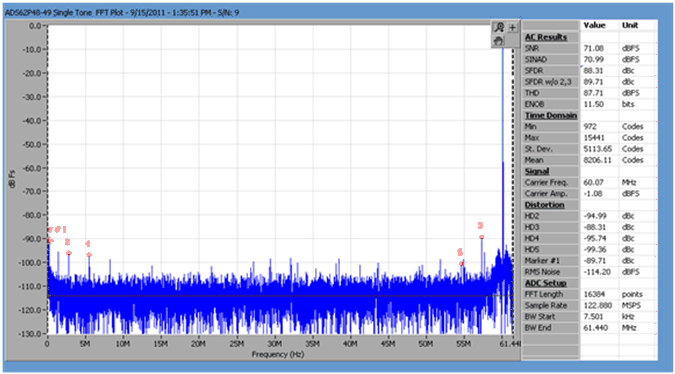 Figure 52. IF = 60 MHz Fclk = 122.88 MHz CDCM6208V2G driving ADC
Observation: up to an IF = 100 MHz, The ADC performance when driven by the CDCM6208V2G (Figure 52) is similar to when the ADC is driven by an expensive lab signal generator with additional passive source filtering (Figure 51).
Conclusion Therefore, the CDCM6208V2G is usable for applications up to 100 MHz IF. For IF above 100 MHz, the SNR starts degrading in our experiments. Measurements were conducted with ADC connected to Y0 and other outputs running at different integer frequencies.
Important note on crosstalk: it is highly recommended that both pre-dividers are configured identically, as otherwise SFDR and SNR suffer due to crosstalk between the two pre-divider frequencies.
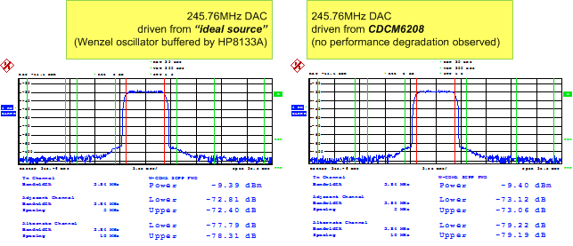 Figure 53. DAC Driven by Lab Source and CDCM6208V2G in Comparison (Performance Identical)
Observation/Conclusion: The DAC performance was not degraded at all by the CDCM6208V2G compared to driving the DAC with a perfect lab source. Therefore, the CDCM6208V2G provides sufficient low noise to drive a 245.76 MHz DAC.
11.2.3 Application Performance Plots
11.2.3.1 Typical Device Jitter
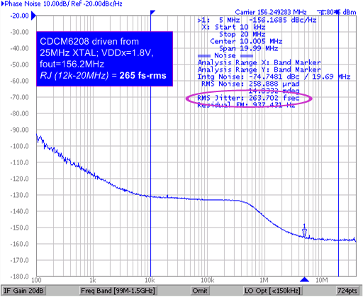 Figure 54. Typical Device Output Phase Noise and Jitter for 25 MHz
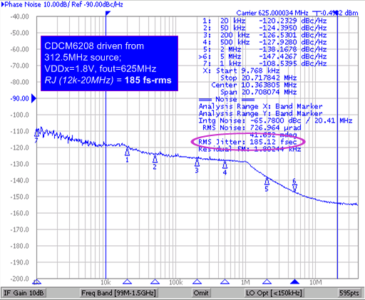 Figure 55. Typical Device Output Phase Noise and Jitter for 312.5 MHz
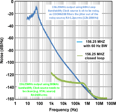 Figure 56. Phase Noise Plot for Jitter Cleaning Mode (blue) and Synthesizer Mode (green)