SGLS390G July 2009 – November 2015 CDCM7005-SP
PRODUCTION DATA.
- 1 Features
- 2 Applications
- 3 Description
- 4 Revision History
- 5 Description (continued)
- 6 Pin Configuration and Functions
- 7 Specifications
- 8 Parameter Measurement Information
-
9 Detailed Description
- 9.1 Overview
- 9.2 Functional Block Diagram
- 9.3 Feature Description
- 9.4 Device Functional Modes
- 9.5 Programming
- 10Application and Implementation
- 11Power Supply Recommendations
- 12Layout
- 13Device and Documentation Support
- 14Mechanical, Packaging, and Orderable Information
10 Application and Implementation
NOTE
Information in the following applications sections is not part of the TI component specification, and TI does not warrant its accuracy or completeness. TI’s customers are responsible for determining suitability of components for their purposes. Customers should validate and test their design implementation to confirm system functionality.
10.1 Application Information
10.1.1 Clock Generation for Interpolating DACs With the CDCM7005-SP
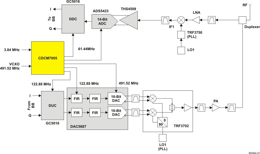
The CDCM7005-SP, with its specified phase noise performance, is an ideal sampling clock generator for high speed ADCs and DACs. The CDCM7005-SP is especially of interest for the new high speed DACs, which have integrated interpolation filter. Such DACs achieve sampling rates up to 500 MSPS. This high data rate can typically not be supported from the digital side driving the DAC (for example, DUC, digital up-converter). Therefore, one approach to interface the DUC to the DAC is the integration of an interpolation filter within the DAC to reduce the data rate at the digital input of the DAC. In 3G systems, for example, a common sampling rate of a high speed DAC is 491.52 MSPS. With a four times interpolation of the digital data, the required input data rate results into 122.88 MSPS, which can be supported easily from the digital side. The DUC GC5016, which supports up to four WCDMA carriers, provides a maximum output data rate of 150 MSPS. An example is shown in Figure 25, where the CDCM7005-SP supplies the clock signal for the DUC/DDC and ADC/DAC.
 Figure 25. CDCM7005-SP as a Clock Generator for High Speed ADCs and DACs
The generation of the two required clock signals (data input clock, clock for DAC) for such an interpolating DAC can be done in different ways. The recommended way is to use the CDCM7005-SP, which generates the fast sampling clock for the DAC from the data input clock signal. The DAC5687 demands that the edges of the two input clocks must be phase aligned within ±500 ps for latching the data properly. This phase alignment is well achieved with the CDCM7005-SP, which assures a maximum skew of 70 ps of the different outputs to each other.
10.1.1.1 AC-Coupled Interface to ADC/DAC
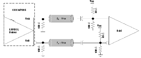
Another advantage of this clock solution is that the ADC or DAC can be driven directly in an ac-coupling interface as shown in Figure 26, with an external termination in a differential configuration. There is no need for a transformer to generate a differential signal from a single-ended clock source.
 Figure 26. Driving DAC or ADC With PECL Output of the CDCM7005-SP
10.1.2 Phase Noise Performance
Table 16. Phase Noise Performance
| PARAMETER(1) | TEST CONDITIONS | REF_IN PHASE NOISE AT 30.72 MHz |
VCXO PHASE NOISE AT 245.76 MHz |
Yx PHASE NOISE AT 30.72 MHz | UNIT | ||
|---|---|---|---|---|---|---|---|
| LVCMOS | LVPECL | ||||||
| TYP(2) | TYP(2) | ||||||
| phn10 | Phase noise at 10 Hz | Y = 30.72 MHz; ƒPFD = 200 kHz, Loop BW = 20 Hz, Feedback Divider = 8 × 128 (N × P), ƒREF_IN = 30.72 MHz, M-Divider = 128, ICP = 2 mA | –109 | –75 | –104 | –100 | dBc/Hz |
| phn100 | Phase noise at 100 Hz | –125 | –97 | –116 | –116 | dBc/Hz | |
| phn1k | Phase noise at 1 kHz | –134 | –117 | –140 | –140 | dBc/Hz | |
| phn10k | Phase noise at 10 kHz | –136 | –138 | –153 | –152 | dBc/Hz | |
| phn100k | Phase noise at 100 kHz | –138 | –148 | –156 | –153 | dBc/Hz | |
| phn1Mk | Phase noise at 1 MHz | –144 | –148 | –156 | –153 | dBc/Hz | |
| phn10M | Phase noise at 10 MHz | –144 | –148 | –156 | –153 | dBc/Hz | |
| PLL STABILIZATION TIME | |||||||
| tstabi | PLL stabilization time(3) | Y = 30.72 MHz, ƒPFD = 200 kHz, Loop BW = 20 Hz, Feedback Divider = 8 × 128 (N × P), ƒREF_IN = 30.72 MHz, M-Divider = 128, ICP = 2 mA | 400 | ms | |||
10.1.2.1 In-Band Noise Performance
Table 17. In-Band Noise Performance
| PARAMETER | TEST CONDITIONS | MIN | TYP | MAX | UNIT | |
|---|---|---|---|---|---|---|
| pnin-band | In-band phase noise test conditions | Y = 900 MHz, ƒPFD = 400 kHz, Loop BW = 27 kHz, Feedback Divider = 8 × 282 (N × P), ƒREF_IN = 10 MHz; M-Divider = 25, ICP = 3 mA |
–95 | dBc/Hz | ||
| pnf400 | Phase noise floor at 400 kHz ƒPFD, in-band noise – 20log(feedback div) (1) | –162 | dBc/Hz | |||
| pnf1 | Phase noise floor at 1 Hz ƒPFD, in-band noise – 20log(feedback div) – 10log(ƒPFD)(2) | –218 | dBc/Hz | |||
where:
pnNfloor = normalized phase noise floor in dBc/Hz
PNmeasured = in-band phase noise measurement in dBc/Hz
20log(N+P) = divider ratio of feedback loop
10log(ƒPFD) = PFD update frequency in Hz
10.2 Typical Application
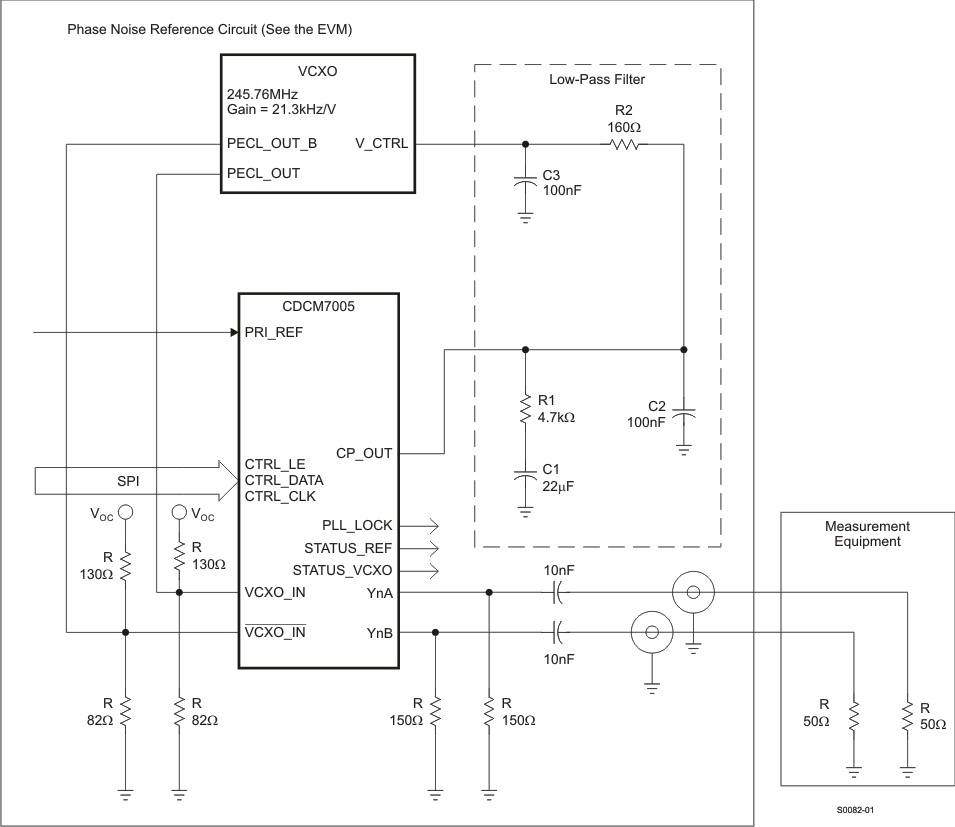
 Figure 27. Typical Application Diagram With Passive Loop Filter
10.2.1 Design Requirements
Before PLL design starts, design targets and constraints should be specified.
Design targets include: output frequency, output phase noise or output jitter over certain band, maximum lock time or maximum dynamic frequency deviation during settling.
Design constraints might include: input frequency, specific VCO/VCXO device, certain type of filter (for example, passive)
Most probably VCO/VCXO is determined based on the noise requirements, or frequency plan needs. Input frequency is typically given by application or system needs. Power or noise requirement might dictate certain type of filter.
10.2.2 Detailed Design Procedure
The CDCM7005-SP design procedure aims at:
- Properly configuring the PLL dividers to achieve lock under given frequency plan
- Determining loop BW/phase margin/gain peaking to achieve given noise/dynamic performance
- Determine the filter type and component values based on the loop BW/phase margin
The proper division ratios can be calculated from the given relations:
- fout: The desired output frequency (240 MHz for LVCMOS, 1.5 GHz max for LVPECL)
- fin: The given input frequency (200 MHz maximum)
- fVCO : The selected VCO or VCXO frequency (2.0 GHz maximum)
- fPFD: The update frequency of the PFD, 100 MHz maximum
- M : Reference divider (10 bits: 1 to 1024)
- P2 : Output divider, also known as Output Mux (/1, /2, /3, /4, /6, /8, /16)
- P1 : Pre-scalar, also known as Feedback Mux (/1, /2, /3, /4, /6, /8, /16)
- N : Feedback divider (12 bits: 1 to 4096), with max input freq of 300 MHz.
Once frequency plan and feasible divider settings are determined, a proper BW/phase margin and gain peaking should be determined. The best way to determine those parameters is to use the TI CDCM7005-SP PLL Calculator tool (PLL-SIM) available on TI website.
Several iterations might be required to achieve the optimum BW/phase margin for a given phase noise and dynamic performance. Better dynamic performance (faster settling) requires higher BW, and possibly some peaking. This is, however, typically increases the phase noise contribution of the PLL and increases frequency offset during settling. Noise performance doesn’t only depend on the loop parameters, but also on the noise performance of the input source and the selected VCO/VCXO. PLL Calculator tool allows the user to include noise profiles from those two sources into noise calculation.
Once the loop parameters are specified, filter design and charge pump current can be determined. CDCM72005 charge pump can be set in the range of 200 µA to 3 mA with 200 µA step. PLL Calculator tool supports filter component value synthesis for three types of filter: second order passive filter, third order passive filter, and third order active filter. Other filter types can be used but the user has to carry out the calculation manually.
Third order pole placement is typically a trade-off between stability and spur performance (spur suppression) the closer the third pole to the loop BW, the higher the suppression, but the phase margin deteriorates and hence loop stability is affected.
Example:
Design a PLL using CDCM7005-SP using an input reference of 10.23 MHz, and VCXO of 155 MHz and an output of the same frequency, using a passive filter.
A common divisor of 10.23 MHz and 155 MHz is 310 kHz which can be used as update frequency.
M = 33, N = 125, P1 = 4, and P2 = 1 should lead to loop lock.
Using the PLL calculator tool, an RMS jitter of 700 ps (given the reference and VCXO noise profile) can be achieved using a loop BW of 1.34 kHz and phase margin of around 80 degrees.
This can be achieved with Charge pump current of 3 mA. The PLL calculator tool can also calculate the filter component values.
10.2.3 Application Curve
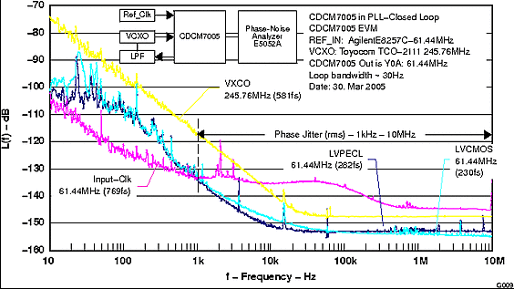
 Figure 28. Phase Noise (61.44-MHz REF_IN and 61.44-MHz Output Frequency)