SGLS390G July 2009 – November 2015 CDCM7005-SP
PRODUCTION DATA.
- 1 Features
- 2 Applications
- 3 Description
- 4 Revision History
- 5 Description (continued)
- 6 Pin Configuration and Functions
- 7 Specifications
- 8 Parameter Measurement Information
-
9 Detailed Description
- 9.1 Overview
- 9.2 Functional Block Diagram
- 9.3 Feature Description
- 9.4 Device Functional Modes
- 9.5 Programming
- 10Application and Implementation
- 11Power Supply Recommendations
- 12Layout
- 13Device and Documentation Support
- 14Mechanical, Packaging, and Orderable Information
8 Parameter Measurement Information
 Figure 10. LVPECL Differential Output Voltage and Rise/Fall Time

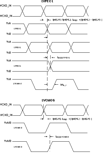
A. Output skew, tsk(o), is calculated as the greater of:
The difference between the fastest and the slowest tpd(LH)n (n = 0...4)
The difference between the fastest and the slowest tpd(HL)n (n = 0...4)
The difference between the fastest and the slowest tpd(LH)n (n = 0...4)
The difference between the fastest and the slowest tpd(HL)n (n = 0...4)
B. Pluse skew, tsk(p), is calculated as the magnitude of the absolute time difference between the high-to-low (tpd(HL)) and the low-to-high (tpd(LH)) propagation delays when a single switching input causes one or more outputs to switch,
tsk(p) = |tpd(HL) – tpd(LH) |. Pulse skew is sometimes refered to as pulse width distortion or duty cycle skew.
Figure 11. Output Skew
tsk(p) = |tpd(HL) – tpd(LH) |. Pulse skew is sometimes refered to as pulse width distortion or duty cycle skew.
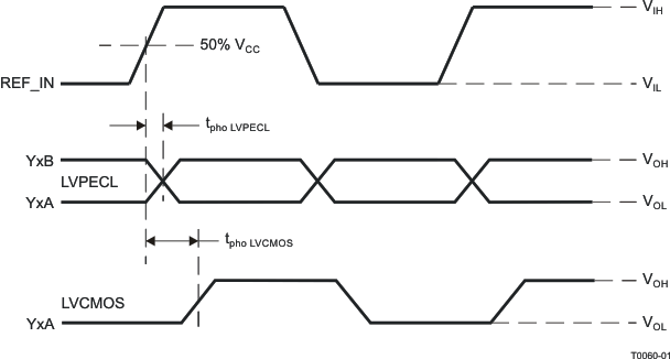
 Figure 12. Phase Offset
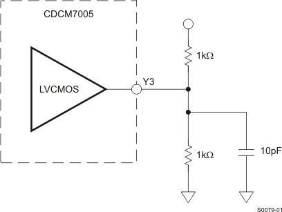
 Figure 13. LVCMOS Output Loading During Device Test
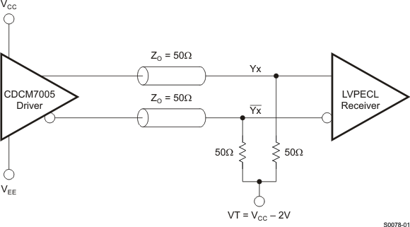
 Figure 14. LVPECL Output Loading During Device Test