ZHCS757A February 2012 – April 2016 CDCM9102
PRODUCTION DATA.
- 1 特性
- 2 应用范围
- 3 说明
- 4 修订历史记录
- 5 Device Comparison Table
- 6 Pin Configuration and Functions
- 7 Specifications
- 8 Parameter Measurement Information
- 9 Detailed Description
- 10Application and Implementation
- 11Power Supply Recommendations
- 12Layout
- 13器件和文档支持
- 14机械、封装和可订购信息
11 Power Supply Recommendations
TA = –40°C to 85°C, VDDx = 3.3 V, OE = 1, values represent cumulative current/power on all VDDx pins.
Table 6. Device Current Consumption
| BLOCK | CONDITION | CURRENT (mA) | DEVICE POWER (mW) | EXTERNAL RESISTOR POWER (mW) |
|---|---|---|---|---|
| Entire device, core current |
85 | 280 | ||
| Output Buffers | LVPECL | 28 | 42.4 | 50 |
| LVDS | 20 | 66 | ||
| LVCMOS | V × ƒout × (CL + 20 × 10–12) × 103 | V2 × ƒout × (CL + 20 × 10–12) × 103 |
11.1 Thermal Management
To ensure optimal performance and reliability, good thermal design practices are important when using the CDCM9102. Die temperature should be limited to a maximum of 125°C. That is, as an estimate, TA (ambient temperature) plus device power consumption times RθJA should not exceed 125°C.
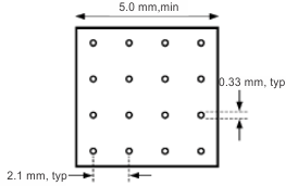
The device package has an exposed pad that provides the primary heat removal path as well as an electrical grounding to the printed circuit board (PCB). To maximize the removal of heat from the package, a thermal landing pattern including multiple vias to a ground plane must be incorporated on the PCB within the footprint of the package. The exposed pad must be soldered down to ensure adequate heat conduction out of the package. A recommended land and via pattern is shown in Figure 19.
 Figure 19. Recommended PCB Layout for CDCM9102
11.2 Power Supply Filtering
PLL-based frequency synthesizers are very sensitive to noise on the power supply, which can dramatically increase the jitter of the PLL. This is especially true for analog-based PLLs. Thus, it is essential to reduce noise from the system power supply, especially when jitter/phase noise is very critical to applications. A PLL has attenuated jitter due to power supply noise at frequencies beyond the PLL bandwidth due to attenuation by the loop response.
Filter capacitors are used to eliminate the low-frequency noise from the power supply, where the bypass capacitors provide the very low-impedance path for high-frequency noise and guard the power supply system against induced fluctuations. The bypass capacitors also provide a source of instantaneous current as required by the device output stages. Therefore, bypass capacitors must have low ESR. To properly use the bypass capacitors, they must be placed very close to the power supply pins and must be laid out with short loops to minimize inductance.
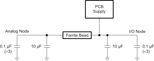
Figure 20 shows a general recommendation for decoupling the power supply. The CDCXM9102 power supplies fall into one of two categories: analog supplies (VDD3, VDD4, and VDD5), and input/output supplies (VDD1, VDD2, and VDD6). Short the analog supplies together to form the analog supply node; likewise, short the input/output supplies together to form the I/O supply node. Isolate the analog node from the PCB power supply and I/O node by inserting a ferrite bead. This helps isolate the high-frequency switching noises generated by the clock drivers and I/O from the sensitive analog supply node. Choosing an appropriate ferrite bead with low dc resistance is important, as it is imperative to maintain a voltage at the power-supply pin of the CDCM9102 that is over the minimum voltage needed for its proper operation.
 Figure 20. CDCM9102 Power Supply Decoupling – Power Pin Bypass Concept