ZHCSG99 April 2017 CDCS504-Q1
PRODUCTION DATA.
9 Application and Implementation
NOTE
Information in the following applications sections is not part of the TI component specification, and TI does not warrant its accuracy or completeness. TI’s customers are responsible for determining suitability of components for their purposes. Customers should validate and test their design implementation to confirm system functionality.
9.1 Application Information
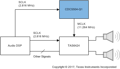
The CDCS504-Q1 is a clock buffer or multiplier for automotive amplifiers and infotainment. It is fit for the TAS6424-Q1, a four-channel, class-D, digital-input audio-amplifier, when the applications are without available MCLK. See Figure 6 for more details.
9.2 Typical Application
 Figure 6. Clock for Automotive Amplifiers
9.2.1 Design Requirements
The CDCS504-Q1 is supplied with a single-power 3.3 V. The device supports minimum input frequency to 2 MHz. For maximum input frequency, it is 32 MHz in ×1 mode, and 27 MHz in ×4 mode. The input clock is LVCMOS type and should satisfy requirements in the Recommended Operating Conditions.
9.2.2 Detailed Design Procedure
In some applications, the clock input for CDCS504-Q1 is not always presented. In case there is an unexpected clock output without clock input, TI recommends setting OE pin to low. When it gets clock input ready, set OE pin to high to get expected clock output. If the other application presents continuous clock input for CDCS504-Q1, the OE pin could be floated, internal pullup brings output enable, or an external pullup circuits could be used fixedly.
9.2.2.1 Custom Design With WEBENCH® Tools
Click here to create a custom design using the CDCS504-Q1 device with the WEBENCH® Power Designer.
- Start by entering the input voltage (VIN), output voltage (VOUT), and output current (IOUT) requirements.
- Optimize the design for key parameters such as efficiency, footprint, and cost using the optimizer dial.
- Compare the generated design with other possible solutions from Texas Instruments.
The WEBENCH Power Designer provides a customized schematic along with a list of materials with real-time pricing and component availability.
In most cases, these actions are available:
- Run electrical simulations to see important waveforms and circuit performance
- Run thermal simulations to understand board thermal performance
- Export customized schematic and layout into popular CAD formats
- Print PDF reports for the design, and share the design with colleagues
Get more information about WEBENCH tools at www.ti.com/WEBENCH.
9.2.3 Application Curves

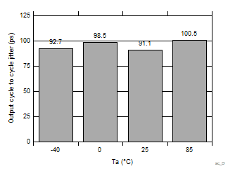
| X1 mode, 8-MHz input, 8-MHz output, VDD = 3.3 V |

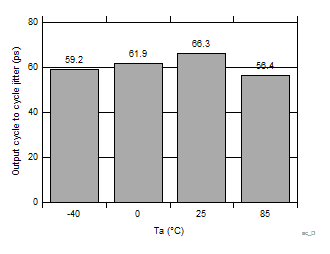
| X4 mode, 27.5-MHz input, 110-MHz output, VDD = 3.3 V |