SLPS260E March   2010  – September 2015 CSD17313Q2

PRODUCTION DATA.  

  1. 1Features
  2. 2Applications
  3. 3Description
  4. 4Revision History
  5. 5 Specifications
    1. 5.1 Electrical Characteristics
    2. 5.2 Thermal Characteristics
    3. 5.3 Typical MOSFET Characteristics
  6. 6Device and Documentation Support
    1. 6.1 Community Resources
    2. 6.2 Trademarks
    3. 6.3 Electrostatic Discharge Caution
    4. 6.4 Glossary
  7. 7Mechanical, Packaging, and Orderable Information
    1. 7.1 Q2 Package Dimensions
    2. 7.2 Recommended PCB Pattern
    3. 7.3 Recommended Stencil Pattern
    4. 7.4 Q2 Tape and Reel Information

封装选项

请参考 PDF 数据表获取器件具体的封装图。

机械数据 (封装 | 引脚)
  • DQK|6
散热焊盘机械数据 (封装 | 引脚)
订购信息

5 Specifications

5.1 Electrical Characteristics

TA = 25°C (unless otherwise noted)
PARAMETER TEST CONDITIONS MIN TYP MAX UNIT
STATIC CHARACTERISTICS
BVDSS Drain-to-source voltage VGS = 0 V, ID = 250 μA 30 V
IDSS Drain-to-source leakage VGS = 0 V, VDS = 24 V 1 μA
IGSS Gate-to-source leakage VDS = 0 V, VGS = +10 / –8 V 100 nA
VGS(th) Gate-to-source threshold voltage VDS = VGS, ID = 250 μA 0.9 1.3 1.8 V
RDS(on) Drain-to-source on resistance VGS = 3 V, ID = 4 A 31 42
VGS = 4.5 V, ID = 4 A 26 32
VGS = 8 V, ID = 4 A 24 30
gfs Transconductance VDS = 15 V, ID = 4 A 16 S
DYNAMIC CHARACTERISTICS
Ciss Input capacitance VGS = 0 V, VDS = 15 V,
ƒ = 1 MHz
260 340 pF
Coss Output capacitance 140 180 pF
Crss Reverse transfer capacitance 13 17 pF
RG Series gate resistance 1.3 2.6 Ω
Qg Gate charge total (4.5 V) VDS = 15 V,
ID = 4 A
2.1 2.7 nC
Qgd Gate charge – gate-to-drain 0.4 nC
Qgs Gate charge – gate-to-source 0.7 nC
Qg(th) Gate charge at Vth 0.3 nC
Qoss Output charge VDS = 13.5 V, VGS = 0 V 3.8 nC
td(on) Turn on delay time VDS = 15 V, VGS = 4.5 V,
ID = 4 A, RG = 2 Ω
2.8 ns
tr Rise time 3.9 ns
td(off) Turn off delay time 4.2 ns
tf Fall time 1.3 ns
DIODE CHARACTERISTICS
VSD Diode forward voltage ISD = 4 A, VGS = 0 V 0.85 1 V
Qrr Reverse recovery charge VDD= 13.5 V, IF = 4 A,
di/dt = 300 A/μs
6.4 nC
trr Reverse recovery time 12.9 ns

5.2 Thermal Characteristics

TA = 25°C (unless otherwise noted)
PARAMETER MIN TYP MAX UNIT
RθJC Thermal resistance junction-to-case(1) 7.4 °C/W
RθJA Thermal resistance junction-to-ambient(1)(2) 67 °C/W
(1) RθJC is determined with the device mounted on a 1 inch2 (6.45 cm2), 2 oz. (0.071 mm thick) Cu pad on a 1.5 inch × 1.5 inch (3.81 cm × 3.81 cm), 0.06 inch (1.52 mm) thick FR4 PCB. RθJC is specified by design, whereas RθJA is determined by the user’s board design.
(2) Device mounted on FR4 material with 1 inch2 (6.45 cm2), 2 oz. (0.071 mm thick) Cu.
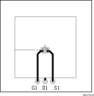
CSD17313Q2 M0179-01_LPS260.gif
Max RθJA = 67°C/W when mounted on 1-inch2 (6.45-cm2) of 2-oz. (0.071-mm thick) Cu.
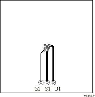
CSD17313Q2 M0180-01_LPS260.gif
Max RθJA = 228°C/W when mounted on a minimum pad area of 2-oz. (0.071-mm thick) Cu.

5.3 Typical MOSFET Characteristics

TA = 25°C (unless otherwise noted)
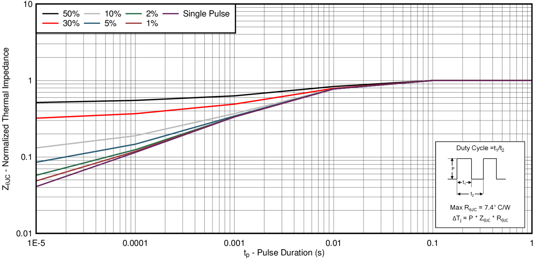
CSD17313Q2 D001_SLPS260.png
Figure 1. Transient Thermal Impedance
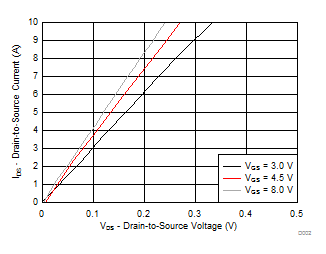
CSD17313Q2 D002_SLPS260_r2.gif
Figure 2. Saturation Characteristics
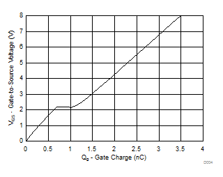
CSD17313Q2 D004_SLPS260.gif
ID = 4 A VDS = 15 V
Figure 4. Gate Charge
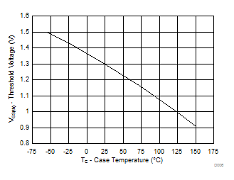
CSD17313Q2 D006_SLPS260.gif
ID = 250 µA
Figure 6. Threshold Voltage vs Temperature
CSD17313Q2 D008_SLPS260.gif
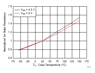
ID = 4 A
Figure 8. Normalized On-State Resistance vs Temperature
CSD17313Q2 D010_SLPS260_r2.gif
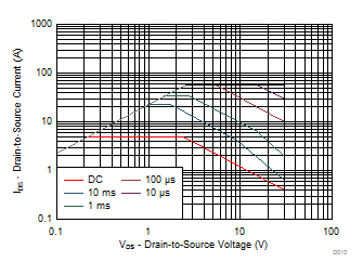
Single Pulse, Max RθJC = 7.4°C/W
Figure 10. Maximum Safe Operating Area
CSD17313Q2 D003_SLPS260.gif
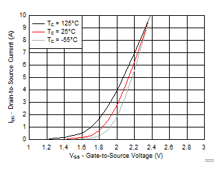
VDS = 5 V
Figure 3. Transfer Characteristics
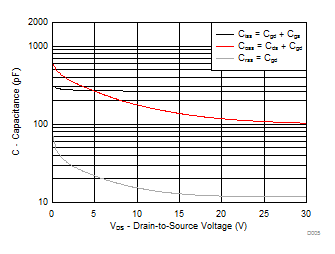
CSD17313Q2 D005_SLPS260.gif
Figure 5. Capacitance
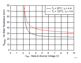
CSD17313Q2 D007_SLPS260.gif
ID = 4 A
Figure 7. On-State Resistance vs Gate-to-Source Voltage
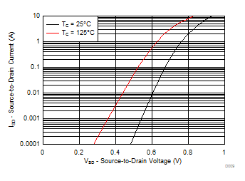
CSD17313Q2 D009_SLPS260.gif
Figure 9. Typical Diode Forward Voltage
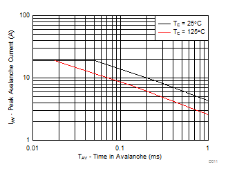
CSD17313Q2 D011_SLPS260.gif
Figure 11. Single Pulse Unclamped Inductive Switching
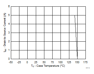
CSD17313Q2 D012_SLPS260.gif
Figure 12. Maximum Drain Current vs Temperature