ZHCS976C June   2012  – June 2015 CSD18503Q5A

PRODUCTION DATA.  

  1. 1特性
  2. 2应用范围
  3. 3说明
  4. 4修订历史记录
  5. 5Specifications
    1. 5.1 Electrical Characteristics
    2. 5.2 Thermal Information
    3. 5.3 Typical MOSFET Characteristics
  6. 6器件和文档支持
    1. 6.1 社区资源
    2. 6.2 商标
    3. 6.3 静电放电警告
    4. 6.4 术语表
  7. 7机械、封装和可订购信息
    1. 7.1 Q5A 封装尺寸
    2. 7.2 建议印刷电路板 (PCB) 布局
    3. 7.3 建议模板开口
    4. 7.4 Q5A 卷带信息

封装选项

机械数据 (封装 | 引脚)
散热焊盘机械数据 (封装 | 引脚)
订购信息

5 Specifications

5.1 Electrical Characteristics

(TA = 25°C unless otherwise stated)
PARAMETER TEST CONDITIONS MIN TYP MAX UNIT
STATIC CHARACTERISTICS
BVDSS Drain to-source voltage VGS = 0 V, ID = 250 μA 40 V
IDSS Drain-to-source leakage current VGS = 0 V, VDS = 32 V 1 μA
IGSS Gate-to-source leakage current VDS = 0 V, VGS = 20 V 100 nA
VGS(th) Gate-to-source threshold voltage VDS = VGS, ID = 250 μA 1.5 1.8 2.3 V
RDS(on) Drain-to-source on-resistance VGS = 4.5 V, ID = 22 A 4.7 6.2
VGS = 10 V, ID = 22 A 3.4 4.3
gfs Transconductance VDS = 20 V, ID = 22 A 100 S
DYNAMIC CHARACTERISTICS
Ciss Input capacitance VGS = 0 V, VDS = 20 V, ƒ = 1 MHz 2200 2640 pF
Coss Output capacitance 510 612 pF
Crss Reverse transfer capacitance 13 16 pF
RG Series gate resistance 1.2 2.4 Ω
Qg Gate charge total (4.5 V) VDS = 20 V, ID = 22 A 13 16 nC
Qg Gate charge total (10 V) 27 32
Qgd Gate charge gate-to-drain 4.3 nC
Qgs Gate charge gate-to-source 4.5 nC
Qg(th) Gate charge at Vth 3.8 nC
Qoss Output charge VDS = 20 V, VGS = 0 V 30 nC
td(on) Turn on delay time VDS = 20 V, VGS = 10 V,
IDS = 22 A, RG = 0
4.5 ns
tr Rise time 8.8 ns
td(off) Turn off delay time 15 ns
tf Fall time 2.6 ns
DIODE CHARACTERISTICS
VSD Diode forward voltage ISD = 22 A, VGS = 0 V 0.8 1 V
Qrr Reverse recovery charge VDS= 20 V, IF = 22 A,
di/dt = 300 A/μs
52 nC
trr Reverse recovery time 37 ns

5.2 Thermal Information

(TA = 25°C unless otherwise stated)
THERMAL METRIC MIN TYP MAX UNIT
RθJC Junction-to-case thermal resistance(1) 1.3 °C/W
RθJA Junction-to-ambient thermal resistance(1)(2) 50 °C/W
(1) RθJC is determined with the device mounted on a 1 inch2 (6.45 cm2), 2 oz. (0.071 mm thick) Cu pad on a 1.5 inch × 1.5 inch
(3.81 cm × 3.81 cm), 0.06 inch (1.52 mm) thick FR4 PCB. RθJC is specified by design, whereas RθJA is determined by the user’s board design.
(2) Device mounted on FR4 material with 1 inch2 (6.45 cm2), 2 oz. (0.071 mm thick) Cu.
CSD18503Q5A M0137-01_LPS198.gif
Max RθJA = 50°C/W when mounted on 1 inch2 (6.45 cm2) of
2 oz. (0.071 mm thick) Cu.
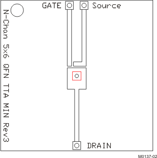
CSD18503Q5A M0137-02_LPS198.gif
Max RθJA = 125°C/W when mounted on a minimum pad area of
2 oz. (0.071 mm thick) Cu.

5.3 Typical MOSFET Characteristics

(TA = 25°C unless otherwise stated)
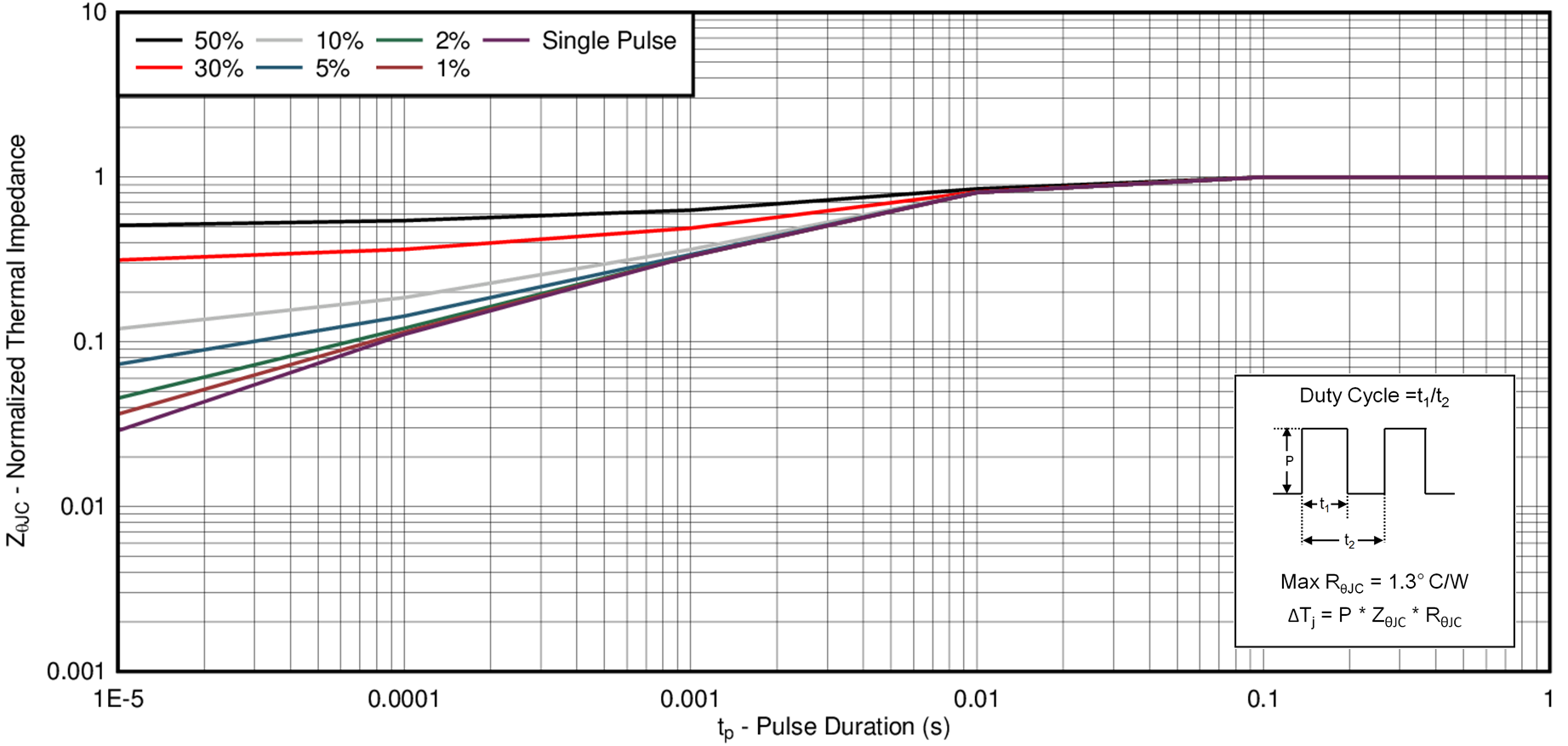
CSD18503Q5A D001_SLPS358.png
Figure 1. Transient Thermal Impedance
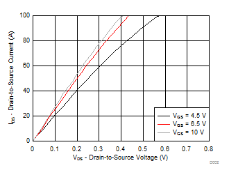
CSD18503Q5A D002_SLPS358.gif
Figure 2. Saturation Characteristics
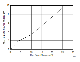
CSD18503Q5A D004_SLPS358.gif
ID = 22 A VDS = 20 V
Figure 4. Gate Charge
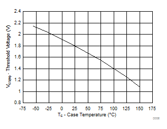
CSD18503Q5A D006_SLPS358.gif
ID = 250 µA
Figure 6. Threshold Voltage vs Temperature
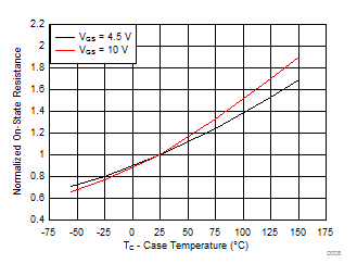
CSD18503Q5A D008_SLPS358.gif
ID = 22 A
Figure 8. Normalized On-State Resistance vs Temperature
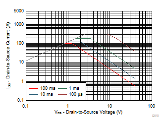
CSD18503Q5A D010_SLPS358.gif
Single Pulse, Max RθJC = 1.3°C/W
Figure 10. Maximum Safe Operating Area
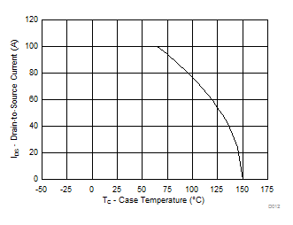
CSD18503Q5A D012_SLPS358.gif
Figure 12. Maximum Drain Current vs Temperature
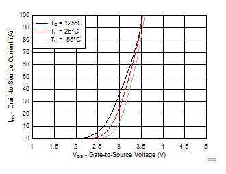
CSD18503Q5A D003_SLPS358.gif
VDS = 5 V
Figure 3. Transfer Characteristics
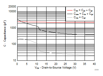
CSD18503Q5A D005_SLPS358.gif
Figure 5. Capacitance
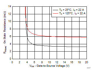
CSD18503Q5A D007_SLPS358.gif
Figure 7. On-State Resistance vs Gate-to-Source Voltage
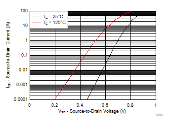
CSD18503Q5A D009_SLPS358.gif
Figure 9. Typical Diode Forward Voltage
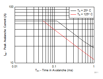
CSD18503Q5A D011_SLPS358.gif
Figure 11. Single Pulse Unclamped Inductive Switching