ZHCSF05 November 2016 TPS25810-Q1
PRODUCTION DATA.
- 1 特性
- 2 应用
- 3 说明
- 4 修订历史记录
- 5 Pin Configuration and Functions
- 6 Specifications
-
7 Detailed Description
- 7.1 Overview
- 7.2 Functional Block Diagram
- 7.3
Feature Description
- 7.3.1 Configuration Channel Pins CC1 and CC2
- 7.3.2 Current Capability Advertisement and Overload Protection
- 7.3.3
Undervoltage Lockout (UVLO)
- 7.3.3.1 Device Power Pins (IN1, IN2, AUX, OUT, and GND)
- 7.3.3.2 FAULT Response
- 7.3.3.3 Thermal Shutdown
- 7.3.3.4 REF
- 7.3.3.5 Audio Accessory Detection
- 7.3.3.6 Debug Accessory Detection
- 7.3.3.7 Plug Polarity Detection
- 7.3.3.8 Device Enable Control
- 7.3.3.9 Load Detect
- 7.3.3.10 Power Wake
- 7.3.3.11 Port Power Management (PPM)
- 7.3.3.12 Implementing PPM in a System With Two Type-C Ports
- 7.3.3.13 PPM Operation
- 7.4 Device Functional Modes
- 8 Application and Implementation
- 9 Power Supply Recommendations
- 10Layout
- 11器件和文档支持
- 12机械、封装和可订购信息
10 Layout
10.1 Layout Guidelines
Layout best practices as they apply to the TPS25810-Q1 device are listed as follows.
- For all applications, a 10-µF ceramic capacitor is recommended near the Type-C receptacle and another 120‑µF ceramic capacitor close to the IN1 pin.
- The optimum placement of the 120-µF capacitor is closest to the IN1 and GND pins of the device.
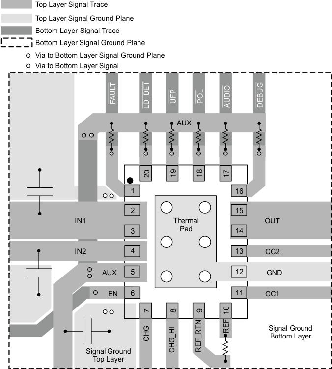
- Care must be taken to minimize the loop area formed by the bypass capacitor connection, the IN1 pin, and the GND pin of the IC. See Figure 29 for a PCB layout example.
- High-current-carrying power-path connections to the device should be as short as possible and should be sized to carry at least twice the full-load current.
- Have the input and output traces as short as possible. The most common cause of voltage loss failure in USB power delivery is the resistance associated with the VBUS trace. Trace length, maximum current being supplied for normal operation, and total resistance associated with the VBUS trace must be taken into account while budgeting for voltage loss.
- For example, a power-carrying trace that supplies 3 A, at a distance of 20 inches, 0.1-in. wide, with 2‑oz. copper on the outer layer has a total resistance of approximately 0.046 Ω and voltage loss of 0.14 V. The same trace at 0.05 in. wide has a total resistance of approximately 0.09 Ω and voltage loss of 0.28 V.
- Make power traces as wide as possible.
- The resistor attached to the REF pin of the device has several requirements:
- It is recommended to use a 1% 100-kΩ low-temperature-cocoefficient resistor.
- It should be connected to the REF and REF_RTN pins (pins 9 and pin 10, respectively).
- The REF_RTN pin should be isolated from the GND plane. See Figure 29.
- The trace routing between the REF and REF_RTN pins of the device should be as short as possible to reduce parasitic effects on current-limit and current-advertisement accuracy. These traces should not have any coupling to switching signals on the board.
- Locate all TPS25810-Q1 pullup resistors for open-drain outputs close to their connection pin. Pullup resistors should be 100 kΩ.
- When a particular open-drain output is not used or needed in the system, leave the associated pin open or tied to GND.
- Keep the CC lines close to the same length.
- Thermal considerations:
- When properly mounted, the thermal-pad package provides significantly greater cooling ability than an ordinary package. To operate at rated power, the thermal pad must be soldered to the board GND plane directly under the device. The thermal pad is at GND potential and can be connected using multiple vias to inner-layer GND. Other planes, such as the bottom side of the circuit board, can be used to increase heat sinking in higher-current applications. See the PowerPad™ Thermally Enhanced Package technical report (SLMA002) and PowerPAD™ Made Easy application brief (SLMA004) for more information on using this thermal pad package.
- The thermal via land pattern specific to the TPS25810-Q1 device can be downloaded from the device Web page at www.ti.com.
- Obtaining acceptable performance with alternate layout schemes is possible; however, the layout example in the following section has been shown to produce good results and is intended as a guideline.
- ESD considerations:
- The TPS25810-Q1 device has built-in ESD protection for CC1 and CC2. Keep trace length to a minimum from the Type-C receptacle to the TPS25810-Q1 device on CC1 and CC2.
- A 10-µF output capacitor should be placed near the Type-C receptacle.
- See the TPS25810EVM-745 evaluation module for an example of a double-layer board that passes IEC61000-4-2 testing.
- Do not create stubs or test points on the CC lines. Keep the traces short if possible, and use minimal vias along the traces (1–2 inches or less).
- See the ESD Protection Layout Guide application report (SLVA680) for additional information.
- Have a dedicated ground plane layer, if possible, to avoid differential voltage buildup.
10.2 Layout Example
 Figure 29. Layout Example