ZHCSGA1 May 2017 CSD22206W
PRODUCTION DATA.
5 Specifications
5.1 Electrical Characteristics
TA = 25°C (unless otherwise stated)| PARAMETER | TEST CONDITIONS | MIN | TYP | MAX | UNIT | ||
|---|---|---|---|---|---|---|---|
| STATIC CHARACTERISTICS | |||||||
| BVDSS | Drain-to-source voltage | VGS = 0 V, IDS = –250 μA | –8 | V | |||
| BVGSS | Gate-to-source voltage | VDS = 0 V, IG = –250 μA | –6 | V | |||
| IDSS | Drain-to-source leakage current | VGS = 0 V, VDS = –6.4 V | –1 | μA | |||
| IGSS | Gate-to-source leakage current | VDS = 0 V, VGS = –6 V | –100 | nA | |||
| VGS(th) | Gate-to-source threshold voltage | VDS = VGS, IDS = –250 μA | –0.4 | –0.7 | –1.05 | V | |
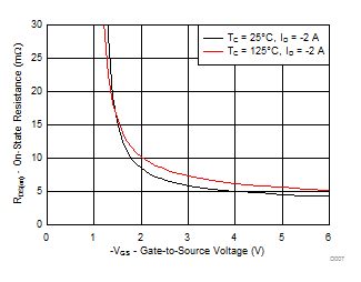
| RDS(on) | Drain-to-source on resistance | VGS = –2.5 V, IDS = –2 A | 6.8 | 9.1 | mΩ | ||
| VGS = –4.5 V, IDS = –2 A | 4.7 | 5.7 | |||||
| gfs | Transconductance | VDS = –0.8 V, IDS = –2 A | 20 | S | |||
| DYNAMIC CHARACTERISTICS | |||||||
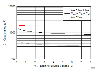
| CISS | Input capacitance | VGS = 0 V, VDS = –4 V, ƒ = 1 MHz |
1750 | 2275 | pF | ||
| COSS | Output capacitance | 960 | 1250 | pF | |||
| CRSS | Reverse transfer capacitance | 340 | 440 | pF | |||
| RG | Series gate resistance | 30 | Ω | ||||
| Qg | Gate charge total (–4.5 V) | VDS = –4 V, ID = –2 A |
11.2 | 14.6 | nC | ||
| Qgd | Gate charge gate-to-drain | 1.8 | nC | ||||
| Qgs | Gate charge gate-to-source | 2.1 | nC | ||||
| Qg(th) | Gate charge at Vth | 1.3 | nC | ||||
| QOSS | Output charge | VDS = –4 V, VGS = 0 V | 7.2 | nC | |||
| td(on) | Turnon delay time | VDS = –4 V, VGS = –4.5 V, IDS = –2 A, RG = 0 Ω |
37 | ns | |||
| tr | Rise time | 17 | ns | ||||
| td(off) | Turnoff delay time | 118 | ns | ||||
| tf | Fall time | 45 | ns | ||||
| DIODE CHARACTERISTICS | |||||||
| VSD | Diode forward voltage | IDS = –2 A, VGS = 0 V | –0.69 | –1.0 | |||
| Qrr | Reverse recovery charge | VDS= –4 V, IF = –1 A, di/dt = 200 A/μs |
24 | nC | |||
| trr | Reverse recovery time | 59 | ns | ||||
5.2 Thermal Information
TA = 25°C (unless otherwise stated)| THERMAL METRIC | TYPICAL VALUES | UNIT | |||
|---|---|---|---|---|---|
| RθJA | Junction-to-ambient thermal resistance(1) | 75 | °C/W | ||
| Junction-to-ambient thermal resistance(2) | 230 | ||||
(1) Device mounted on FR4 material with 1-in2 (6.45-cm2), 2-oz (0.071-mm) thick Cu.
(2) Device mounted on FR4 material with minimum Cu mounting area.
 |
Typ RθJA = 75°C/W when mounted on 1 in2 of 2-oz Cu. |
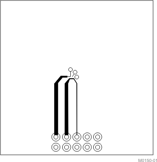 |
Typ RθJA = 230°C/W when mounted on minimum pad area of 2-oz Cu. |
5.3 Typical MOSFET Characteristics
TA = 25°C (unless otherwise stated)


| ID = –2 A | VDS = –4 V | ||
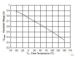
| ID = –250 µA | ||
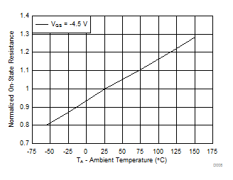
| ID = –2 A | ||
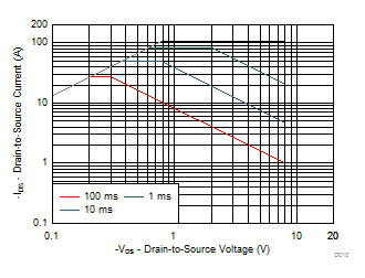
| Single pulse, max RθJA = 75°C/W | ||
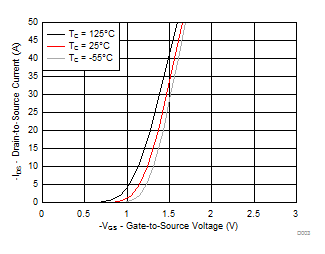
| VDS = –4 V | ||
