SLPS264D October 2010 – May 2015 CSD86330Q3D
PRODUCTION DATA.
9 Mechanical, Packaging, and Orderable Information
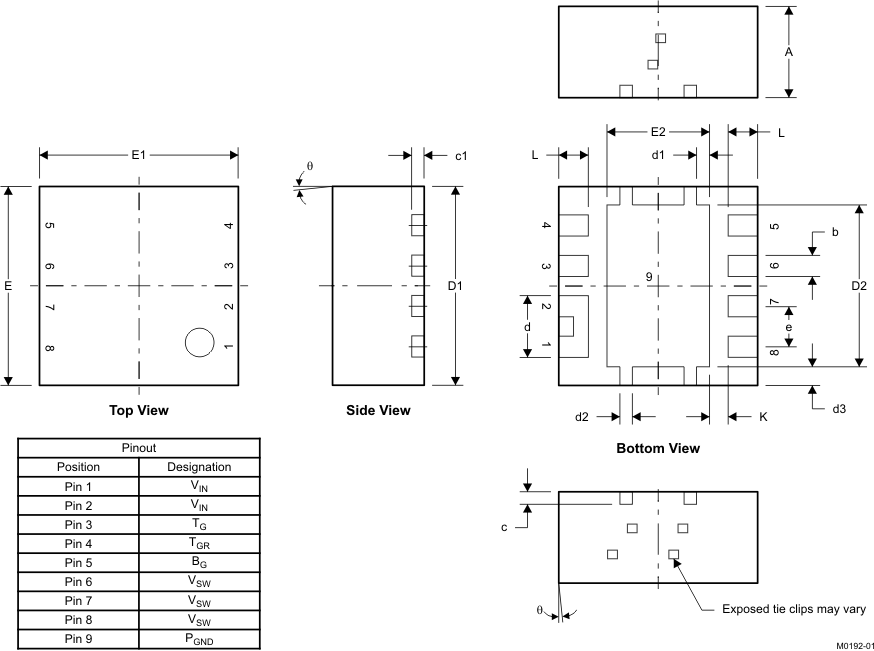
9.1 Q3D Package Dimensions

| DIM | MILLIMETERS | INCHES | ||
|---|---|---|---|---|
| MIN | MAX | MIN | MAX | |
| A | 1.40 | 1.5 | 0.055 | 0.059 |
| b | 0.280 | 0.400 | 0.011 | 0.016 |
| c | 0.150 | 0.250 | 0.006 | 0.010 |
| c1 | 0.150 | 0.250 | 0.006 | 0.010 |
| d | 0.940 | 1.040 | 0.037 | 0.041 |
| d1 | 0.160 | 0.260 | 0.006 | 0.010 |
| d2 | 0.150 | 0.250 | 0.006 | 0.010 |
| d3 | 0.250 | 0.350 | 0.010 | 0.014 |
| D1 | 3.200 | 3.400 | 0.126 | 0.134 |
| D2 | 2.650 | 2.750 | 0.104 | 0.108 |
| E | 3.200 | 3.400 | 0.126 | 0.134 |
| E1 | 3.200 | 3.400 | 0.126 | 0.134 |
| E2 | 1.750 | 1.850 | 0.069 | 0.073 |
| e | 0.650 TYP | 0.026 TYP | ||
| L | 0.400 | 0.500 | 0.016 | 0.020 |
| θ | 0.00 | — | — | — |
| K | 0.300 TYP | 0.012 TYP | ||
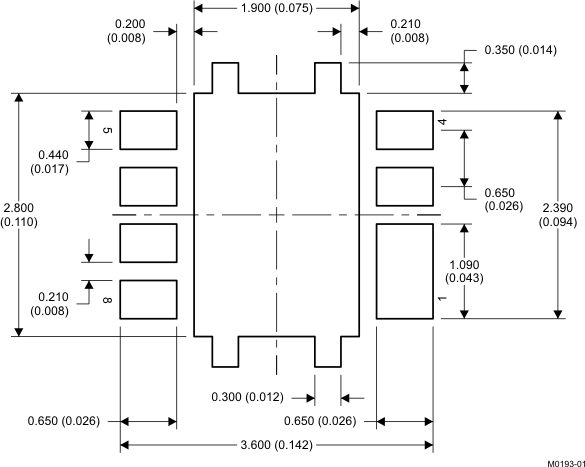
9.2 Land Pattern Recommendation

NOTE:
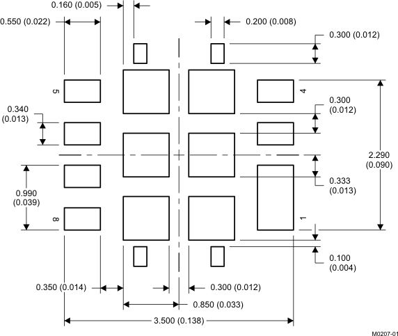
Dimensions are in mm (inches).9.3 Stencil Recommendation

NOTE:
Dimensions are in mm (inches).For recommended circuit layout for PCB designs, see application note SLPA005 – Reducing Ringing Through PCB Layout Techniques.
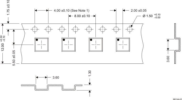
9.4 Q3D Tape and Reel Information

NOTES:
1. 10-sprocket hole-pitch cumulative tolerance ±0.2 2. Camber not to exceed 1 mm in 100 mm, noncumulative over 250 mm
3. Material: black static-dissipative polystyrene
4. All dimensions are in mm, unless otherwise specified.
5. Thickness: 0.30 ±0.0 5 mm
6. MSL1 260°C (IR and convection) PbF reflow compatible