ZHCSHU1 March   2018 CSD86336Q3D

PRODUCTION DATA.  

  1. 1特性
  2. 2应用
  3. 3说明
    1.     俯视图
      1.      Device Images
  4. 4修订历史记录
  5. 5Specifications
    1. 5.1 Absolute Maximum Ratings
    2. 5.2 Recommended Operating Conditions
    3. 5.3 Thermal Information
    4. 5.4 Power Block Performance
    5. 5.5 Electrical Characteristics – Q1 Control FET
    6. 5.6 Electrical Characteristics – Q2 Sync FET
    7. 5.7 Typical Power Block Device Characteristics
    8. 5.8 Typical Power Block MOSFET Characteristics
  6. 6Application and Implementation
    1. 6.1 Application Information
      1. 6.1.1 Equivalent System Performance
    2. 6.2 Power Loss Curves
    3. 6.3 Safe Operating Area (SOA) Curves
    4. 6.4 Normalized Curves
    5. 6.5 Calculating Power Loss and Safe Operating Area (SOA)
      1. 6.5.1 Design Example
      2. 6.5.2 Calculating Power Loss
      3. 6.5.3 Calculating SOA Adjustments
  7. 7Layout
    1. 7.1 Recommended Schematic Overview
    2. 7.2 Recommended PCB Design Overview
      1. 7.2.1 Electrical Performance
      2. 7.2.2 Thermal Performance
  8. 8器件和文档支持
    1. 8.1 接收文档更新通知
    2. 8.2 社区资源
    3. 8.3 商标
    4. 8.4 静电放电警告
    5. 8.5 Glossary
  9. 9机械、封装和可订购信息
    1. 9.1 Q3D 封装尺寸
    2. 9.2 引脚配置
    3. 9.3 焊盘图案建议
    4. 9.4 模版建议

封装选项

机械数据 (封装 | 引脚)
散热焊盘机械数据 (封装 | 引脚)
订购信息

Typical Power Block Device Characteristics

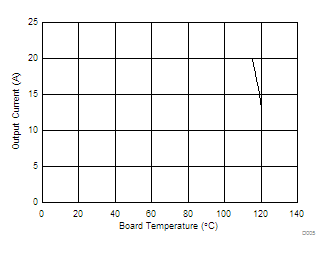
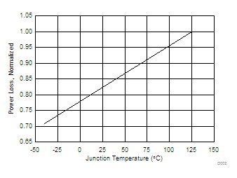
Test conditions: VIN = 12 V, VDD = 5 V, ƒSW = 500 kHz, VOUT = 1.3 V, LOUT = 0.95 µH, IOUT = 20 A, TJ = 125°C, unless stated otherwise.
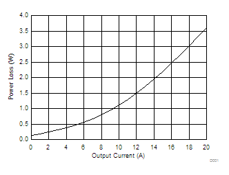
CSD86336Q3D D001_SLPS666.gif
Figure 1. Power Loss vs Output Current
CSD86336Q3D D005_SLPS666.gif
Figure 3. Typical Safe Operating Area (SOA) (1)
CSD86336Q3D D002_SLPS666.gif
Figure 2. Power Loss vs Temperature
CSD86336Q3D D006_SLPS666.gif
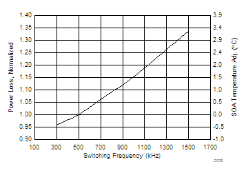
Figure 4. Normalized Power Loss vs Switching Frequency
CSD86336Q3D D008_SLPS666.gif
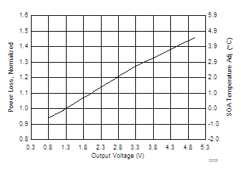
Figure 6. Normalized Power Loss vs Output Voltage
CSD86336Q3D D007_SLPS666.gif
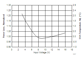
Figure 5. Normalized Power Loss vs Input Voltage
CSD86336Q3D D009_SLPS666.gif
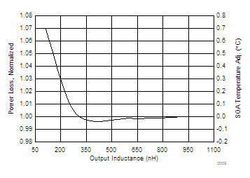
Figure 7. Normalized Power Loss vs Output Inductance
The Typical Power Block System Characteristic curves are based on measurements made on a PCB design with dimensions of 4 in (W) × 3.5 in (L) × 0.062 in (H) and 6 copper layers of 1-oz copper thickness. See Application and Implementation section for detailed explanation.