ZHCSAE5B September   2012  – April 2018 CSD86360Q5D

PRODUCTION DATA.  

  1. 1特性
  2. 2应用
  3. 3说明
    1. 3.1 俯视图
      1.      Device Images
  4. 4修订历史记录
  5. 5Specifications
    1. 5.1 Absolute Maximum Ratings
    2. 5.2 Recommended Operating Conditions
    3. 5.3 Power Block Performance
    4. 5.4 Thermal Information
    5. 5.5 Electrical Characteristics
    6. 5.6 Typical Power Block Device Characteristics
    7. 5.7 Typical Power Block MOSFET Characteristics
  6. 6Application and Implementation
    1. 6.1 Application Information
      1. 6.1.1 Equivalent System Performance
      2. 6.1.2 Power Loss Curves
      3. 6.1.3 Safe Operating Area (SOA) Curves
      4. 6.1.4 Normalized Curves
    2. 6.2 Typical Application
      1. 6.2.1 Design Example: Calculating Power Loss and SOA
        1. 6.2.1.1 Operating Conditions
        2. 6.2.1.2 Calculating Power Loss
        3. 6.2.1.3 Calculating SOA Adjustments
  7. 7Layout
    1. 7.1 Layout Guidelines
      1. 7.1.1 Electrical Performance
      2. 7.1.2 Thermal Performance
    2. 7.2 Layout Example
  8. 8器件和文档支持
    1. 8.1 文档支持
      1. 8.1.1 相关文档
    2. 8.2 接收文档更新通知
    3. 8.3 社区资源
    4. 8.4 商标
    5. 8.5 静电放电警告
    6. 8.6 术语表
  9. 9机械、封装和可订购信息
    1. 9.1 Q5D 封装尺寸
    2. 9.2 焊盘布局建议
    3. 9.3 模版建议
    4. 9.4 Q5D 卷带信息

封装选项

机械数据 (封装 | 引脚)
散热焊盘机械数据 (封装 | 引脚)
订购信息

Typical Power Block Device Characteristics

TJ = 125°C, unless stated otherwise.
CSD86360Q5D graph01p2_SLPS287.png
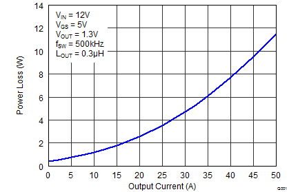
Figure 1. Power Loss vs Output Current
CSD86360Q5D graph03pe_SLPS327.png
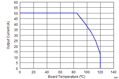
Figure 3. Safe Operating Area – PCB Vertical Mount (1)1
CSD86360Q5D graph05_SLPS287.png
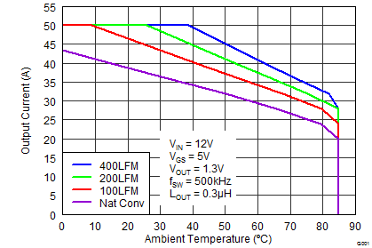
Figure 5. Typical Safe Operating Area(1)1
CSD86360Q5D graph02_SLPS223.png
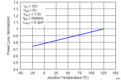
Figure 2. Normalized Power Loss vs Temperature
CSD86360Q5D graph04p3_SLPS327.png
Figure 4. Safe Operating Area – PCB Horizontal Mount (1)1
The Typical Power Block System Characteristic curves are based on measurements made on a PCB design with dimensions of 4 in (W) × 3.5 in (L) × 0.062 in (H) and 6 copper layers of 1-oz copper thickness. See Application and Implementation section for detailed explanation.
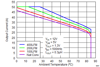
CSD86360Q5D graph06_SLPS327.png
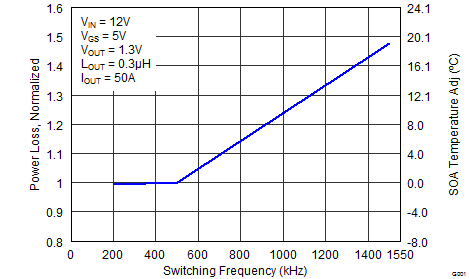
Figure 6. Normalized Power Loss vs Switching Frequency
CSD86360Q5D graph08_SLPS327.png
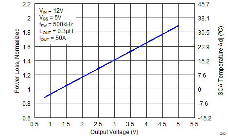
Figure 8. Normalized Power Loss vs Output Voltage
CSD86360Q5D graph07p2_SLPS327.png
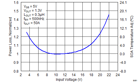
Figure 7. Normalized Power Loss vs Input Voltage
CSD86360Q5D graph09_SLPS327.png
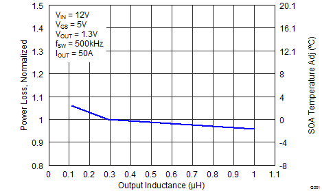
Figure 9. Normalized Power Loss vs Output Inductance