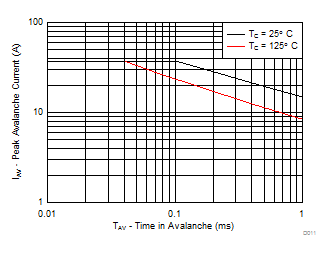
ZHCSG72 April 2017 CSD87313DMS
PRODUCTION DATA.
5 Specifications
5.1 Electrical Characteristics
TA = 25°C (unless otherwise stated)| PARAMETER | TEST CONDITIONS | MIN | TYP | MAX | UNIT | ||
|---|---|---|---|---|---|---|---|
| STATIC CHARACTERISTICS | |||||||
| IS1S2 | Source1-to-Source2 leakage current | VG1S1 = 0 V, VG2S2 = 0 V, VS1S2 = 24 V | 1 | μA | |||
| IGSS | Gate-to-source leakage current | VS1S2 = 0 V, VGS = 10 V | 100 | nA | |||
| VGS(th) | Gate-to-source threshold voltage | VS1S2 = VGS, IS1S2 = 250 μA | 0.6 | 0.9 | 1.2 | V | |
| RS1S2(on) | Source1-to-Source2 on resistance | VGS = 2.5 V, IS1S2 = 20 A | 6.7 | 9.6 | mΩ | ||
| VGS = 4.5 V, IS1S2 = 23 A | 4.6 | 5.5 | |||||
| gfs | Transconductance | VS1S2 = 3 V, IS1S2 = 23 A | 149 | S | |||
| DYNAMIC CHARACTERISTICS(1) | |||||||
| CISS | Input capacitance | VGS = 0 V, VS1S2 = 15 V, ƒ = 1 MHz | 3300 | 4290 | pF | ||
| COSS | Output capacitance | 281 | 365 | pF | |||
| CRSS | Reverse transfer capacitance | 154 | 200 | pF | |||
| Qg | Gate charge total (4.5 V) | VS1S2 = 15 V, IS1S2 = 23 A VG1S1 = 4.5 V, VG2S2 = 0 V |
28 | nC | |||
| Qgd | Gate charge gate-to-drain | 6.0 | nC | ||||
| Qgs | Gate charge gate-to-source | 6.3 | nC | ||||
| Qg(th) | Gate charge at Vth | 3.2 | nC | ||||
| td(on) | Turnon delay time | VS1S2 = 15 V, IS1S2 = 23 A VGS = 4.5 V, RGEN = 0 Ω |
9 | ns | |||
| tr | Rise time | 27 | ns | ||||
| td(off) | Turnoff delay time | 41 | ns | ||||
| tf | Fall time | 13 | ns | ||||
| DIODE CHARACTERISTICS | |||||||
| Ifss | Maximum continuous Source1-to-Source2 diode forward current(2) | VG1S1 = 0 V, VG2S2 = 4.5 V | 2 | A | |||
| Vfss | Source1-to-Source2 diode forward voltage | VG1S1 = 0 V, VG2S2 = 4.5 V, Ifss = 23 A | 0.8 | 1.0 | V | ||
(1) Dynamic characteristic measurements are for a single FET.
(2) Typical RθJA = 125°C/W on a minimum 2-oz Cu pad.
5.2 Thermal Information
TA = 25°C (unless otherwise stated)| THERMAL METRIC | UNIT | ||||
|---|---|---|---|---|---|
| RθJA | Junction-to-case thermal resistance(1) | 125 | °C/W | ||
| RθJA | Junction-to-ambient thermal resistance(1)(2) | 45 | °C/W | ||
(1) Device mounted on minimum 2-oz (0.071-mm) thick Cu.
(2) Device mounted on FR4 material with 1-in2 (6.45-cm2), 2-oz (0.071-mm) thick Cu.
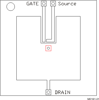 |
RθJA = 45°C/W when mounted on 1 in2 (6.45 cm2) of 2-oz (0.071-mm) thick Cu. |
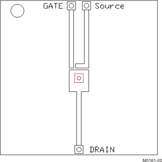 |
RθJA = 125°C/W when mounted on a minimum pad area of 2-oz (0.071-mm) thick Cu. |
5.3 Typical MOSFET Characteristics
TA = 25°C (unless otherwise stated)
| Pulse width = 250 µs, duty cycle = 0.5% | VG2S2 = 4.5 V |
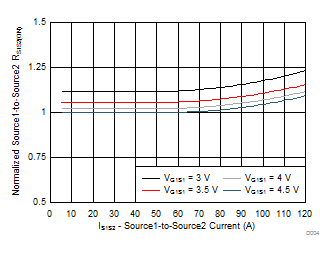
| Pulse width = 250 µs, duty cycle = 0.5% | VG2S2 = 4.5 V |

| IS1S2 = 23 A | VGS = 15 V |

| VS1S2 = 5 V |
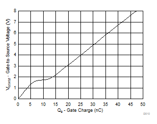
| ID = 23 A | VS1S2 = 15 V |

| Single pulse, RθJA = 125°C/W |

| ID = 250 µA |

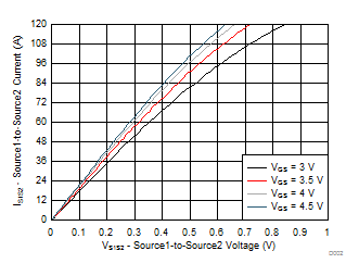
| Pulse width = 250 µs, duty cycle = 0.5% |
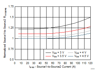
| Pulse width = 250 µs, duty cycle = 0.5% |


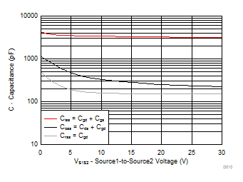

| RθJA = 125 °C/W, TA = 25°C |
