-
CSD87588N 同步降压 NexFET 电源块 II
CSD87588N 同步降压 NexFET 电源块 II
1 特性
2 应用范围
- 同步降压转换器
- 高电流、低占空比应用
- 多相位同步降压转换器
- 负载点 (POL) 直流 - 直流转换器
3 说明
此 CSD87588N NexFET™ 电源块 II 是针对同步降压应用的高度优化设计,能够在 5 mm × 2.5mm 的小外形尺寸封装内提供大电流和高效率。 针对 5V 栅极驱动应用进行了优化,这款米6体育平台手机版_好二三四可提供高效且灵活的解决方案,在与外部控制器/驱动器的任一 5V 栅极驱动器成对使用时,均可提一个供高密度电源。
增加文本,调节间距
订购信息(1)
| 器件 | 介质 | 数量 | 封装 | 出货 |
|---|---|---|---|---|
| CSD87588N | 13 英寸卷带 | 2500 | 5 x 2.5 LGA | 卷带封装 |
| CSD87588NT | 7 英寸卷带 | 250 |
- 要了解所有可用封装,请见数据表末尾的可订购米6体育平台手机版_好二三四附录。
增加文本,调节间距
典型电路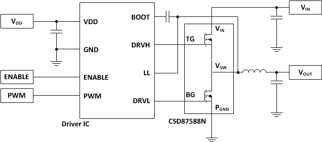 |
典型电源块效率与功率损耗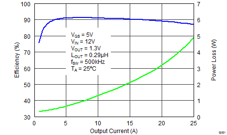 |
4 修订历史记录
Changes from C Revision (June 2014) to D Revision
- Changed capacitance units to read pF in Figure 15Go
- Changed capacitance units to read pF in Figure 16Go
Changes from B Revision (January 2014) to C Revision
- 将“无铅引脚镀层”更改成了“无铅”Go
Changes from A Revision (May 2013) to B Revision
- 已添加小卷带信息Go
- Updated Figure 5Go
- Updated Figure 6Go
- Updated Figure 7Go
- Updated Figure 8Go
- Changed figure reference to Figure 29 in electrical performanceGo
Changes from * Revision (March 2013) to A Revision
- Changed RθJC-PCBTo: RθJC in the Thermal Information tableGo
5 Specifications
5.1 Absolute Maximum Ratings
TA = 25°C (unless otherwise noted) (1)| MIN | MAX | UNIT | |||
|---|---|---|---|---|---|
| Voltage | VIN to PGND | –0.8 | 30 | V | |
| VSW to PGND | 30 | ||||
| VSW to PGND (10 ns) | 32 | ||||
| TG to VSW | –20 | 20 | |||
| BG to PGND | –20 | 20 | |||
| IDM | Pulsed Current Rating(2) | 50 | A | ||
| PD | Power Dissipation(3) | 6 | W | ||
| EAS | Avalanche Energy | Sync FET, ID = 45, L = 0.1 mH | 101 | mJ | |
| Control FET, ID = 26, L = 0.1 mH | 34 | ||||
| TJ | Operating Junction | –55 | 150 | °C | |
| Tstg | Storage Temperature Range | –55 | 150 | °C | |
absolute-maximum-rated conditions for extended periods may affect device reliability.
5.2 Recommended Operating Conditions
TA = 25°C (unless otherwise noted)| MIN | MAX | UNIT | |||
|---|---|---|---|---|---|
| VGS | Gate Drive Voltage | 4.5 | 16 | V | |
| VIN | Input Supply Voltage | 24 | V | ||
| ƒSW | Switching Frequency | CBST = 0.1 μF (min) | 200 | 1500 | kHz |
| Operating Current | No Airflow | 25 | A | ||
| With Airflow (200 LFM) | 30 | A | |||
| With Airflow + Heat Sink | 35 | A | |||
| TJ | Operating Temperature | 125 | °C | ||
5.3 Thermal Information
TA = 25°C (unless otherwise stated)| THERMAL METRIC | MIN | TYP | MAX | UNIT | |
|---|---|---|---|---|---|
| RθJA | Junction-to-ambient thermal resistance (Min Cu) (1) | 170 | °C/W | ||
| Junction-to-ambient thermal resistance (Max Cu) (2)(1) | 70 | ||||
| RθJC | Junction-to-case thermal resistance (Top of package) (1) | 3.7 | |||
| Junction-to-case thermal resistance (PGND Pin) (1) | 1.25 | ||||
(3.81 cm × 3.81 cm), 0.06 inch (1.52 mm) thick FR4 board. RθJC is specified by design while RθJA is determined by the user’s board design.
5.4 Power Block Performance
TA = 25°C (unless otherwise noted)| PARAMETER | CONDITIONS | MIN | TYP | MAX | UNIT | |
|---|---|---|---|---|---|---|
| PLOSS | Power Loss(1) | VIN = 12 V, VGS = 5 V VOUT = 1.3 V, IOUT = 15 A ƒSW = 500 kHz LOUT = 0.29 µH, TJ = 25ºC |
2.1 | W | ||
| IQVIN | VIN Quiescent Current | TG to TGR = 0 V BG to PGND = 0 V |
10 | µA | ||
5.5 Electrical Characteristics
TA = 25°C (unless otherwise stated)| PARAMETER | TEST CONDITIONS | Q1 FET | Q2 FET | UNIT | ||||||
|---|---|---|---|---|---|---|---|---|---|---|
| MIN | TYP | MAX | MIN | TYP | MAX | |||||
| STATIC CHARACTERISTICS | ||||||||||
| BVDSS | Drain-to-Source Voltage | VGS = 0 V, IDS = 250 μA | 30 | 30 | V | |||||
| IDSS | Drain-to-Source Leakage Current | VGS = 0 V, VDS = 24 V | 1 | 1 | μA | |||||
| IGSS | Gate-to-Source Leakage Current | VDS = 0 V, VGS = 20 | 100 | 100 | nA | |||||
| VGS(th) | Gate-to-Source Threshold Voltage | VDS = VGS, IDS = 250 μA | 1.1 | 1.9 | 1.1 | 1.9 | V | |||
| RDS(on) | Drain-to-Source On Resistance | VGS = 4.5 V, IDS = 15 A | 10.4 | 12.5 | 3.5 | 4.2 | mΩ | |||
| VGS = 10 V, IDS = 15 A | 8 | 9.6 | 2.9 | 3.5 | ||||||
| gƒs | Transconductance | VDS = 10 V, IDS = 15 A | 43 | 93 | S | |||||
| DYNAMIC CHARACTERISTICS | ||||||||||
| CISS | Input Capacitance (1) | VGS = 0 V, VDS = 15 V, ƒ = 1 MHz |
566 | 736 | 2310 | 3000 | pF | |||
| COSS | Output Capacitance (1) | 341 | 444 | 682 | 887 | pF | ||||
| CRSS | Reverse Transfer Capacitance (1) | 10.3 | 13.4 | 62 | 80.4 | pF | ||||
| RG | Series Gate Resistance (1) | 1.2 | 2.4 | 1.1 | 2.2 | Ω | ||||
| Qg | Gate Charge Total (4.5 V) (1) | VDS = 15 V, IDS = 15 A |
3.2 | 4.1 | 13.7 | 17.9 | nC | |||
| Qgd | Gate Charge - Gate-to-Drain | 0.7 | 4.3 | nC | ||||||
| Qgs | Gate Charge - Gate-to-Source | 1.4 | 4.3 | nC | ||||||
| Qg(th) | Gate Charge at Vth | 0.8 | 2.8 | nC | ||||||
| QOSS | Output Charge | VDD = 12 V, VGS = 0 V | 7 | 18.6 | nC | |||||
| td(on) | Turn On Delay Time | VDS = 15 V, VGS = 4.5 V, IDS = 15 A, RG = 2 Ω |
7.3 | 12.1 | ns | |||||
| tr | Rise Time | 31.6 | 36.7 | ns | ||||||
| td(off) | Turn Off Delay Time | 10.2 | 20.1 | ns | ||||||
| tƒ | Fall Time | 5.0 | 6.3 | ns | ||||||
| DIODE CHARACTERISTICS | ||||||||||
| VSD | Diode Forward Voltage | IDS = 15 A, VGS = 0 V | 0.85 | 0.78 | V | |||||
| Qrr | Reverse Recovery Charge | Vdd = 15 V, IF = 15 A, di/dt = 300 A/μs |
12.5 | 26.7 | nC | |||||
| trr | Reverse Recovery Time | 16 | 23 | ns | ||||||
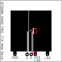 |
Max RθJA = 70°C/W when mounted on 1 inch2 (6.45 cm2) of 2 oz. (0.071 mm thick) Cu. |
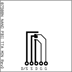 |
Max RθJA = 170°C/W when mounted on minimum pad area of 2 oz. (0.071 mm thick) Cu. |
5.6 Typical Power Block Device Characteristics
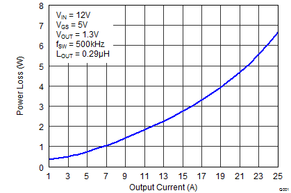
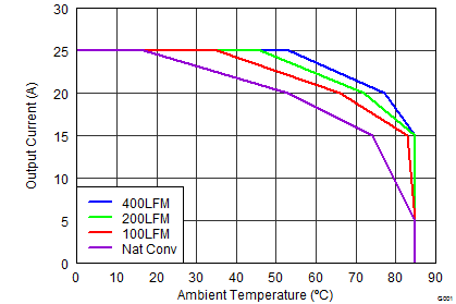
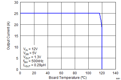
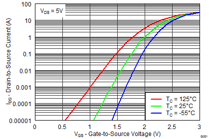
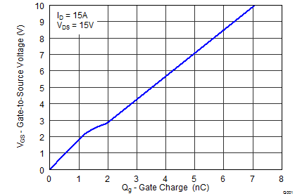
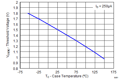
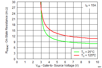
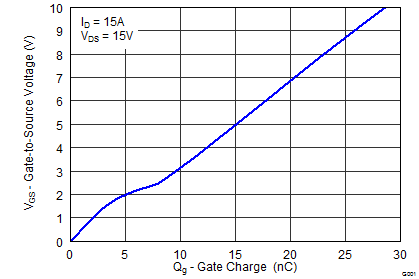
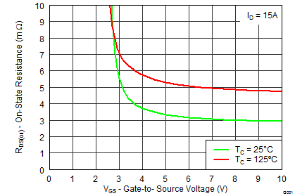
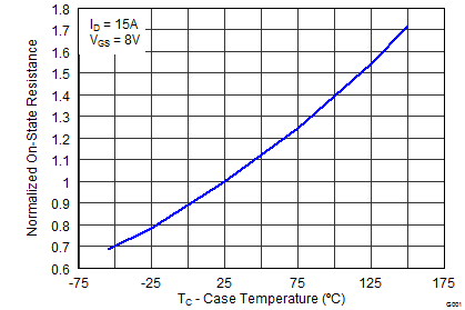
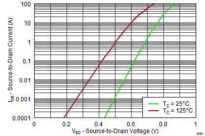
TJ = 125°C, unless stated otherwise.The Typical Power Block System Characteristic curves Figure 3 and Figure 4 are based on measurements made on a PCB design with dimensions of 4.0 inches (W) × 3.5 inches (L) × 0.062 inch (H) and 6 copper layers of 1 oz. copper thickness. See Application and Implementation for detailed explanation.5.7 Typical Power Block MOSFET Characteristics
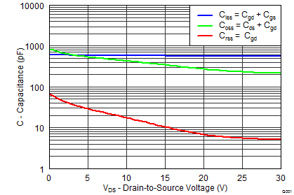
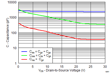
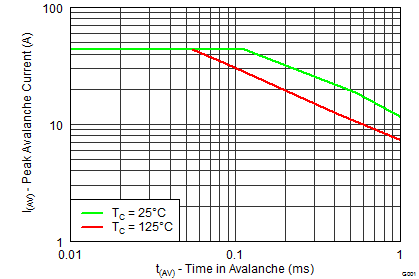
TA = 25°C, unless stated otherwise.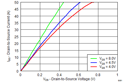


6 Application and Implementation
6.1 Application Information
The CSD87588N NexFET power block is an optimized design for synchronous buck applications using 5 V gate drive. The Control FET and Sync FET silicon are parametrically tuned to yield the lowest power loss and highest system efficiency. As a result, a new rating method is needed which is tailored toward a more systems-centric environment. System-level performance curves such as Power Loss, Safe Operating Area, and normalized graphs allow engineers to predict the product performance in the actual application.
6.1.1 Power Loss Curves
MOSFET-centric parameters such as RDS(ON) and Qgd are needed to estimate the loss generated by the devices. To simplify the design process for engineers, TI has provided measured power loss performance curves. Figure 1 plots the power loss of the CSD87588N as a function of load current. This curve is measured by configuring and running the CSD87588N as it would be in the final application (see Figure 27). The measured power loss is the CSD87588N loss and consists of both input conversion loss and gate drive loss. Equation 1 is used to generate the power loss curve.
The power loss curve in Figure 1 is measured at the maximum recommended junction temperatures of 125°C under isothermal test conditions.
6.1.2 Safe Operating Curves (SOA)
The SOA curves in the CSD87588N data sheet provide guidance on the temperature boundaries within an operating system by incorporating the thermal resistance and system power loss. Figure 3 to Figure 4 outline the temperature and airflow conditions required for a given load current. The area under the curve dictates the safe operating area. All the curves are based on measurements made on a PCB design with dimensions of 4 inches (W) × 3.5 inches (L) × 0.062 inch (T) and 6 copper layers of 1 oz. copper thickness.
6.1.3 Normalized Curves
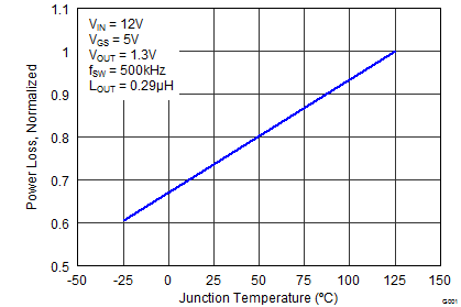
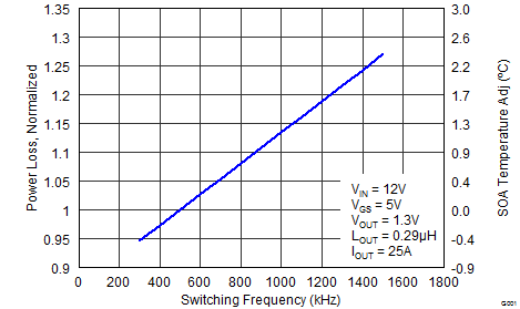
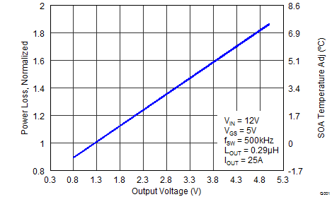
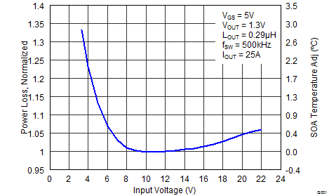
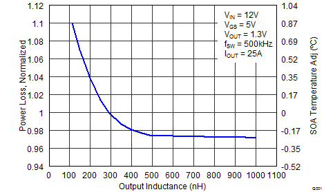
The normalized curves in the CSD87588N data sheet provides guidance on the Power Loss and SOA adjustments based on their application-specific needs. These curves show how the power loss and SOA boundaries adjust for a given set of systems conditions. The primary y-axis is the normalized change in power loss and the secondary y-axis is the change in system temperature required in order to comply with the SOA curve. The change in power loss is a multiplier for the Power Loss curve and the change in temperature is subtracted from the SOA curve.
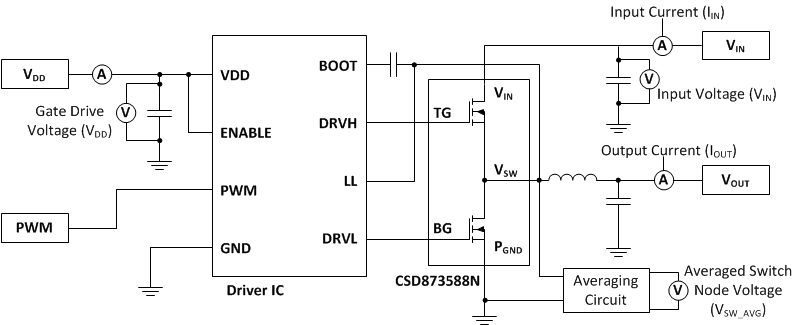 Figure 27. Typical Application
6.1.4 Calculating Power Loss and SOA
The user can estimate product loss and SOA boundaries by arithmetic means (see Design Example). Though the Power Loss and SOA curves in this data sheet are taken for a specific set of test conditions, the following procedure outlines the steps the user should take to predict product performance for any set of system conditions.
6.1.4.1 Design Example
Operating Conditions:
- Output Current = 15 A
- Input Voltage = 7 V
- Output Voltage = 1 V
- Switching Frequency = 800 kHz
- Inductor = 0.2 µH
6.1.4.2 Calculating Power Loss
- Power Loss at 15 A = 2.75 W (Figure 1)
- Normalized Power Loss for input voltage ≈ 1.03 (Figure 6)
- Normalized Power Loss for output voltage ≈ 0.94 (Figure 7)
- Normalized Power Loss for switching frequency ≈ 1.08 (Figure 5)
- Normalized Power Loss for output inductor ≈ 1.03 (Figure 8)
- Final calculated Power Loss = 2.75 W × 1.05 × 0.95 × 1.05 × 1.05 ≈ 3.02 W
6.1.4.3 Calculating SOA Adjustments
In the previous design example, the estimated power loss of the CSD87588N would increase to 3.02 W. In addition, the maximum allowable board and/or ambient temperature would have to decrease by 0.8ºC. Figure 28 graphically shows how the SOA curve would be adjusted accordingly.
- Start by drawing a horizontal line from the application current to the SOA curve.
- Draw a vertical line from the SOA curve intercept down to the board/ambient temperature.
- Adjust the SOA board/ambient temperature by subtracting the temperature adjustment value.
In the design example, the SOA temperature adjustment yields a reduction in allowable board/ambient temperature of 0.8ºC. In the event the adjustment value is a negative number, subtracting the negative number would yield an increase in allowable board/ambient temperature.
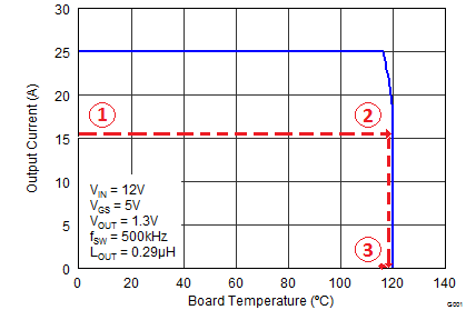 Figure 28. Power Block SOA
